filmov
tv
Formation and Properties of Junction Diode - Physics

Показать описание
This is a physics video for Grade 11-12 students about p-n junction diode, its properties, characteristics and uses. The combination of p-type and n-type semiconductors results in a junction. When a p-type semiconductor is joined with n-type semiconductor, the resultant junction formed is called a p-n junction diode.
 0:02:44
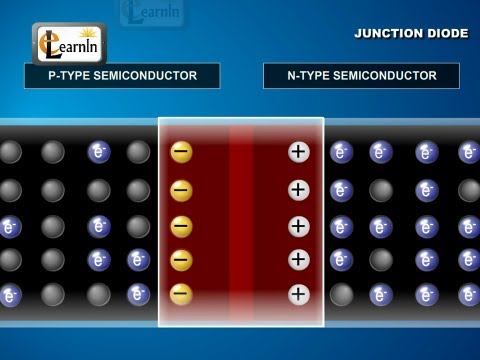
Formation and Properties of Junction Diode - Physics
 0:14:50
PN junction Diode Explained | Forward Bias and Reverse Bias
 0:12:44
Semiconductors, Insulators & Conductors, Basic Introduction, N type vs P type Semiconductor
 0:11:32
Diodes Explained - The basics how diodes work working principle pn junction
 0:10:06
The PN junction | Class 12 (India) | Physics | Khan Academy
 0:03:14
P-N JUNCTION
 0:15:13
How Diodes Are Formed (Semiconductors, PN junction)
 0:22:18
FORMATION OF PN JUNCTION | SEMICONDUCTOR DEVICES | SEMICONDUCTOR ELECTRONICS | PHYSICS COMPANION
 0:27:56
Formation & Properties of P-N Junction Diode
 0:23:44
S1-M1-S9: PN Junction formation via Alloying, Forward and reverse biasing of PN Junction
 0:01:01
What is PN Junction Diode?
 0:18:48
PN Junction diode- Formation and properties | FEEL SIMPLE |
 0:08:44
FORMATION OF THE PN JUNCTION AND IT'S PROPERTIES. episode 3
 0:10:21
PN Junction : An Introducton to basic concepts and properties of pn junction .
 0:04:11
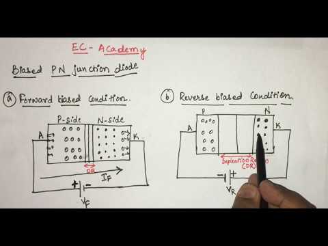
#3 P N junction diode under forward bias and reverse bias Condition || EC Academy
 0:00:55
Cell Junctions - Amoeba Sisters #Shorts
 0:10:04
Metal Semiconductor Junctions | Schottky and Ohmic Junctions | B. Tech/ M. Sc.
 0:08:36
Lecture 41; pn junction; Junction formation 1
 0:02:07
Formation of PN Junction | Unbiased PN Junction | Electron diffusion | Hole diffusion
 0:23:43
Formation of PN junction Diod | Thier Properties....
 0:00:45
Formation of Depletion layer
 0:06:30
PN Junction Diode Construction and Working | Forward Bias and Reverse Bias | Basics of Electronics
 0:00:15
Working of Diodes in Forward & Reverse Bias #Diodes
 0:00:42
How a Muscle Contracts | Muscle Physiology 101
Комментарии