filmov
tv
P-N JUNCTION

Показать описание
For more information:
Contact: +91- 9700061777,
040-64501777 / 65864777
7 Active Technology Solutions Pvt.Ltd. is an educational 3D digital content provider for K-12. We also customize the content as per your requirement for companies platform providers colleges etc . 7 Active driving force "The Joy of Happy Learning" -- is what makes difference from other digital content providers. We consider Student needs, Lecturer needs and College needs in designing the 3D & 2D Animated Video Lectures. We are carrying a huge 3D Digital Library ready to use.
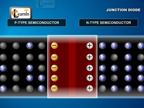
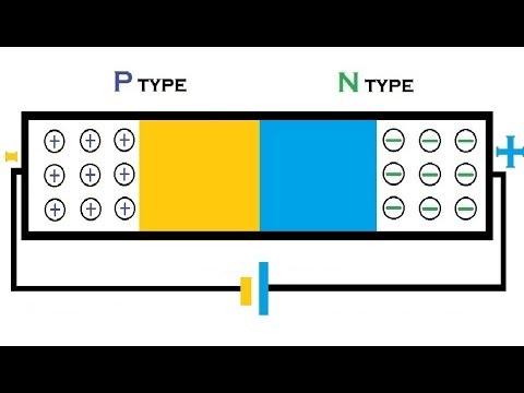
P-N JUNCTION: When a p-type semiconductor is suitably joined to n-type semiconductor, the contact surface in called p-n junction. Consider two types of materials: One p-type and the other n-type as show in diagram. Left side material is a p-type semiconductor ‘having negative acceptor’ ions and positively changed holes. The right side material is n-type semiconductor having positive donor ions and free electrons. Suppose the two pieces are suitably treated to form PN junction. Keep in mind that n- type material has a high concentration of free electrons while p- type material has a high concentration of holes. Therefore, at the junction, there in a tendency for the free electrons to diffuse over to the p-side and holes to the n-side.
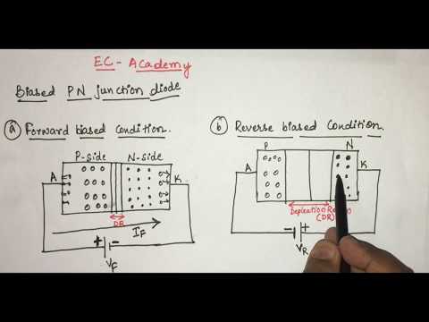
As the free electrons move across the junction from n-type to p-type, positive donor ions are uncovered is they are robbed of free electrons, Hence, a positive charge is built on n-side of the junction. At the same time, the free electrons cross the junction and uncover the negative acceptor ions by filling in the holes. Therefore, a net negative charge in established on P-side of the junction. When a sufficient number of donor and acceptor ions is uncovered, further diffusion is prevented. It is because now positive charge on n-side repels holes to cross from p-type to n- type and negative charge on p-side repels free electron to enter from n-type to p-type. Thus, a barrier is set up against further movement of charge carrier, i.e. holes and electrons. This is called potential barrier or junction barrier v0 The layer name the p-n junction in which no free electrons or holes are available is called the depletion layer.
Contact: +91- 9700061777,
040-64501777 / 65864777
7 Active Technology Solutions Pvt.Ltd. is an educational 3D digital content provider for K-12. We also customize the content as per your requirement for companies platform providers colleges etc . 7 Active driving force "The Joy of Happy Learning" -- is what makes difference from other digital content providers. We consider Student needs, Lecturer needs and College needs in designing the 3D & 2D Animated Video Lectures. We are carrying a huge 3D Digital Library ready to use.
P-N JUNCTION: When a p-type semiconductor is suitably joined to n-type semiconductor, the contact surface in called p-n junction. Consider two types of materials: One p-type and the other n-type as show in diagram. Left side material is a p-type semiconductor ‘having negative acceptor’ ions and positively changed holes. The right side material is n-type semiconductor having positive donor ions and free electrons. Suppose the two pieces are suitably treated to form PN junction. Keep in mind that n- type material has a high concentration of free electrons while p- type material has a high concentration of holes. Therefore, at the junction, there in a tendency for the free electrons to diffuse over to the p-side and holes to the n-side.
As the free electrons move across the junction from n-type to p-type, positive donor ions are uncovered is they are robbed of free electrons, Hence, a positive charge is built on n-side of the junction. At the same time, the free electrons cross the junction and uncover the negative acceptor ions by filling in the holes. Therefore, a net negative charge in established on P-side of the junction. When a sufficient number of donor and acceptor ions is uncovered, further diffusion is prevented. It is because now positive charge on n-side repels holes to cross from p-type to n- type and negative charge on p-side repels free electron to enter from n-type to p-type. Thus, a barrier is set up against further movement of charge carrier, i.e. holes and electrons. This is called potential barrier or junction barrier v0 The layer name the p-n junction in which no free electrons or holes are available is called the depletion layer.
 0:03:14
P-N JUNCTION
 0:05:03
How does a diode work - the PN Junction (with animation) | Intermediate Electronics
 0:14:50
PN junction Diode Explained | Forward Bias and Reverse Bias
 0:11:32
Diodes Explained - The basics how diodes work working principle pn junction
 0:09:59
PN Junction Introduction
 0:02:44
Formation and Properties of Junction Diode - Physics
 0:10:06
The PN junction | Class 12 (India) | Physics | Khan Academy
 0:06:37
Animation | How a P N junction semiconductor works | forward reverse bias | diffusion drift current
 0:03:50
What is Doping in Semiconductor | PN Junction Diode
 0:05:34
Semiconductors 2: the p-n junction (Higher Physics)
 0:14:06
Diodes - What Are Diodes - PN Junction - Forward Bias - Reverse Bias - Zener Diodes
 0:04:11
#3 P N junction diode under forward bias and reverse bias Condition || EC Academy
 0:06:50
Forward biasing a PN junction | Class 12 (India) | Physics | Khan Academy
 0:02:35
What is p-n Junction Diode | Forward Bias & Reverse Bias | Electronic Devices & Circuits
 0:07:50
PN Junction Band Diagram
 0:07:36
How does a P-N Junction Diode works? Explained through Animation
 0:15:53
Class 12th – P-N Junction (Diode) | Semiconductors | Tutorials Point
 0:11:33
55. PN Junction Diode | Semi Conductors | Physics Baba 2.0
 0:33:57
p-n junction under equilibrium
 0:07:49
P-N Junction Diode || 3D animated explanation || class 12th physics|| Semiconductors ||
 0:23:03
Electronic Devices: pn junction under equilibrium - depletion width, build-in potential
 0:08:48
PN Junction Diode | Depletion Region | Potential Barrier | Role of Potential Barrier | Electronics
 0:01:01
What is PN Junction Diode?
 0:04:46
Formation of P-N Junctions - Semiconductor Devices - Applied Physics - MSBTE | Ekeeda.com
Комментарии