filmov
tv
Dynamic Random Access Memory (DRAM). Part 7: Memory Address Mapping

Показать описание
This is the seventh in a series of videos is about the fundamental principles of Dynamic Random Access Memory, DRAM, and the essential concepts of DRAM operation. This video illustrates how the individual bits of a memory address can be allocated among rows, columns and banks in order to control the interleaving of data bursts across multiple banks inside a single chip.
 0:10:28
Dynamic Random Access Memory (DRAM). Part 1: Memory Cell Arrays
 0:04:22
Dynamic Random Acess Memory (DRAM) Explained | 'All About Semiconductor' by Samsung Semico...
 0:35:33
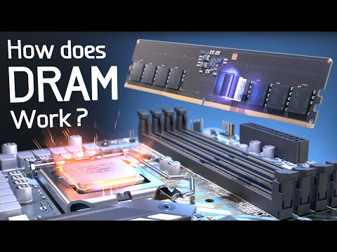
How does Computer Memory Work? 💻🛠
 0:14:25
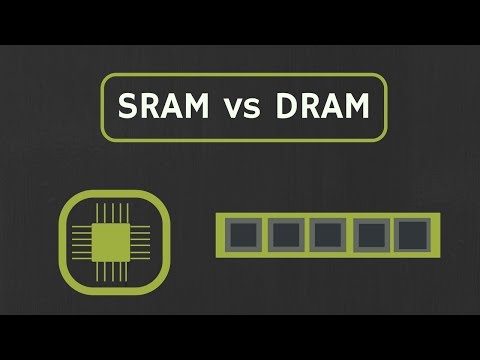
SRAM vs DRAM : How SRAM Works? How DRAM Works? Why SRAM is faster than DRAM?
 0:07:38
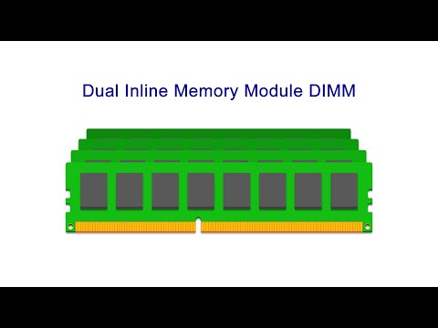
Dynamic Random Access Memory (DRAM). Part 5: DIMM Organisation
 0:10:36
Dynamic Random Access Memory (DRAM). Part 2: Read and Write Cycles
 0:04:58
Static RAM and Dynamic RAM Explained
 0:15:42
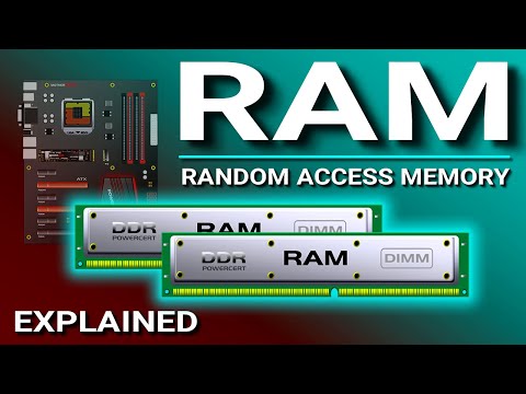
RAM Explained - Random Access Memory
 0:00:12
Dynamic Ram #viralshort #computernetwork # #rrbjeelectrical
 0:12:10
Dynamic Random Access Memory (DRAM). Part 6: Burst Mode and Bank Interleaving
 0:05:51
Dynamic Random Access Memory (DRAM). Part 7: Memory Address Mapping
 0:08:41
Dynamic Random Access Memory (DRAM). Part 4: Multiplexers and Demultiplexers
 0:03:50
Dynamic Random Access Memory (DRAM). Part 3: Binary Decoders
 0:03:15
| Industry Data Analytics | IDA Dynamic Random Access Memory (DRAM) Market
 0:00:39
Dynamic Random Access Memory (DRAM) Market Size and Share Analysis: Key Growth Trends and Projection
 0:01:32
What is DRAM? How is it Different From SRAM?
 0:00:08
Intel introduced the world's first commercially available dynamic random-access memory (DRAM)
 0:00:10
What is DRAM (Dynamic random access memory | Computer Fundamentals |
 0:04:14
One Memory Bit SRAM - Georgia Tech - HPCA: Part 4
 0:00:06
DRAM Dynamic Random Access Memory
 1:30:59
ETH Lecture 02. Dynamic Random Access Memory (DRAM) (24/02/2017)
 0:05:05
How computer memory works - Kanawat Senanan
 0:04:09
CO44 - Dynamic RAMs
 0:15:46
Different Types of DRAM: SDRAM/DDR1/DDR2/DDR3/DDR4/LPDDR/GDDR
Комментарии