filmov
tv
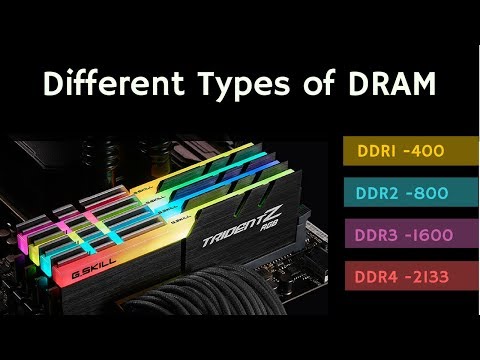
Different Types of DRAM: SDRAM/DDR1/DDR2/DDR3/DDR4/LPDDR/GDDR

Показать описание
In this video, different generations of Dynamic RAM (DRAM) has been compared in terms of their speed/bandwidth and power consumption, in terms of the memory packages (SIMM, DIMM, and SO-DIMM) and in terms of the types of applications in which they are used. In this video, it has been also discussed that how higher speed has been achieved in each generation over the previous generation.
Asynchronous DRAM:
In this type of RAM, the RAM is not synchronized with the CPU Clock.
Synchronous DRAM (SDRAM):
In this type of RAM, the RAM is synchronized with the CPU clock.
It is also known as the Single Data Rate SDRAM, as data is being transferred on the rising edge of every clock pulse.
DDR SDRAM (Double Data Rate SDRAM):
In this type of RAM, the data is transferred twice during each clock cycle, with rising and falling edge.
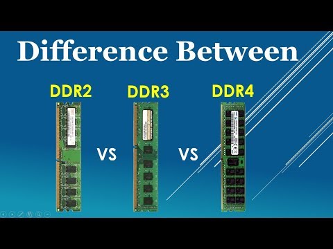
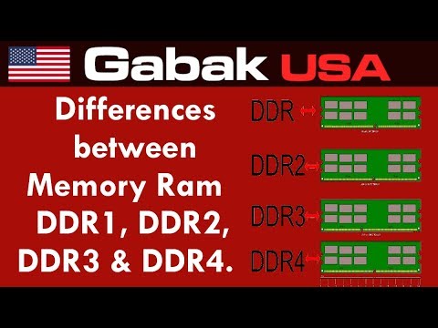
Different Generations of DDR RAMs are DDR1/DDR2/DDR3/DDR4. In each generation of DDR RAM, the speed of the RAM was increased and power consumption has been reduced.
RAM Packages:
DIP (Dual In LIne Package)
SIMM (Single In line Modules)
DIMM (Dual In Line Module)
SO-DIMM (Small Outline DIMM)
Mobile DDR / Low Power DDR (MDDR/LPDDR)
This type of RAM is used inside the smartphones, which is optimized for the low power consumption.
Graphics DDR (GDDR):
This type of RAM is used in graphics cards for multimedia applications which required very high bandwidth.
Timestamps for the different topics in the video:
1:25 Asynchronous DRAM
1:48 Synchronous DRAM (SDRAM)
4:51 DDR1
6:45 DDR2
8:43 DDR3
10:17 DDR4
12:22 SIMM (Single Inline Module)
12:58 DIMM (Dual Inline Module)
13:40 SO-DIMM
14:20 MDDR/LPDDR
15:03 GDDR
This video will be helpful to all the students of science and engineering in understanding the different types of DRAM.
Follow me on YouTube:
Follow me on Facebook:
Follow me on Instagram:
Music Credit:
Asynchronous DRAM:
In this type of RAM, the RAM is not synchronized with the CPU Clock.
Synchronous DRAM (SDRAM):
In this type of RAM, the RAM is synchronized with the CPU clock.
It is also known as the Single Data Rate SDRAM, as data is being transferred on the rising edge of every clock pulse.
DDR SDRAM (Double Data Rate SDRAM):
In this type of RAM, the data is transferred twice during each clock cycle, with rising and falling edge.
Different Generations of DDR RAMs are DDR1/DDR2/DDR3/DDR4. In each generation of DDR RAM, the speed of the RAM was increased and power consumption has been reduced.
RAM Packages:
DIP (Dual In LIne Package)
SIMM (Single In line Modules)
DIMM (Dual In Line Module)
SO-DIMM (Small Outline DIMM)
Mobile DDR / Low Power DDR (MDDR/LPDDR)
This type of RAM is used inside the smartphones, which is optimized for the low power consumption.
Graphics DDR (GDDR):
This type of RAM is used in graphics cards for multimedia applications which required very high bandwidth.
Timestamps for the different topics in the video:
1:25 Asynchronous DRAM
1:48 Synchronous DRAM (SDRAM)
4:51 DDR1
6:45 DDR2
8:43 DDR3
10:17 DDR4
12:22 SIMM (Single Inline Module)
12:58 DIMM (Dual Inline Module)
13:40 SO-DIMM
14:20 MDDR/LPDDR
15:03 GDDR
This video will be helpful to all the students of science and engineering in understanding the different types of DRAM.
Follow me on YouTube:
Follow me on Facebook:
Follow me on Instagram:
Music Credit:
 0:15:46
Different Types of DRAM: SDRAM/DDR1/DDR2/DDR3/DDR4/LPDDR/GDDR
 0:02:36
A Comprehensive Guide to DDR1, DDR2, DDR3, DDR4, and DDR5 RAM Explained
 0:03:48
DDR2 vs DDR3 vs DDR4 Explained Feature and Identify comparison
 0:12:09
differences between ddr1 ddr2 ddr3 & ddr4 and their features
 0:05:37
RAM Evolution Unveiled - How Each Generation Changed the Game
 0:00:10
Types of RAM |
 0:02:25
Difference Between DDR DDR2 DDR3 Desktop RAM Memory
 0:02:43
Differents Between DDR1 DDR2 DDR3 Ram
 0:00:16
DDR (Dual Data Rate) 4
 0:01:28
WHAT ARE THE TYPES OF LAPTOP RAM? - SDRAM-DDR-DDR2-DDR3-DDR4-DDR5
 0:00:09
Difference between SDRAM and DDR SDRAM 0? #differencebetween #class #
 0:27:29
RAM (Random Access Memory) Types, Functions, DDR, How much RAM needed, Trends, Before buying a RAM,
 0:04:02
SDRAM / DDR-SDRAM / DDR2-SDRAM / DDR3-SDRAM
 0:00:09
different types DDR3 rams #shorts #ddr3 #ram
 0:01:41
What is the difference between DDR2 and DDR3 RAM?
 0:21:11
DDR-DDR2-DDR3-DDR4
 0:14:58
DDR Memory
 0:00:32
DDR 4 RAM | What Is Random Access Memory (RAM) #laptop #shorts #youtubeshort #2022
 0:00:19
Brand new DDR1?! #shorts #howtotech #retrotech #gamingpc #gaming #gamerguy #gamergirl
 0:00:16
DYNAMIC Synchronous RAM and Small Outline Dual Inline Memory Module.
 0:00:09
difference between SDRAM and DDR
 0:00:18
How to find different of RAM DDR1 DDR2 DDR3 DDR4 in 3 second
 0:04:10
HOW MUCH SPEED? WHAT IS RAM | DDR1, DDR2, DDR3, DDR4
 0:00:54
EDO, Fast Page, SDRAM, DDR, DDR2, DDR3, and Laptop Memory in antistatic bags. #shorts
Комментарии