filmov
tv
DDR3 data byte, Address, Command & Control routine
Показать описание
DDR3 data byte, Address, Command & Control routine
Jakhang's Electronics
Рекомендации по теме
0:05:10
DDR3 data byte, Address, Command & Control routine
0:26:39
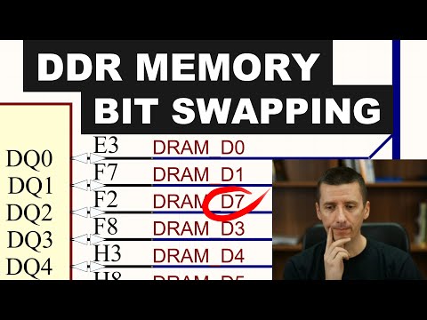
How to Do DDR Memory Bit & Byte Swapping - DDR2, DDR3, DDR4, ....
0:14:51
Solving DDR Memory Challenges with Advanced Simulation
0:00:21
The Easiest Way To Check Your PC RAM
0:06:15
Defining and routing PCB constraints for DDR3 memory circuits - Part 1: The theory
0:05:51
Dynamic Random Access Memory (DRAM). Part 7: Memory Address Mapping
0:06:30
DDR (double data rate) Signals || DQ, DQS, CK, Address, clock, control & command signals
0:01:19
SDR to DDR SDRAM -- DLL timing
0:15:00
DDR3 2133 Tutorial Intro
0:25:43
FPGA/SoC Board Bring-Up - DDR3 (Zynq Part 2) - Phil's Lab #97
0:04:31
PolarFire® FPGA & PolarFire® SOC DDR PHY Initialization and Training Sequence for DRAM Interface...
1:25:37
DDR protocol training demo session
0:12:10
Dynamic Random Access Memory (DRAM). Part 6: Burst Mode and Bank Interleaving
0:53:20
What You Need to Know When Routing DDR3 Part 1 of 2
0:43:22
ECC'17: DDR3 memory initialization basics on Intel Sandybrige platforms
0:14:58
DDR Memory
0:03:36
DDR Memory Test Solutions Overview
0:03:15
Electronics: Data Strobe in DDR memory (2 Solutions!!)
1:20:08
How To Measure DDR Memories? (DDR5 / DDR4 / DDR3)
0:03:17
xSignals for DDR3 and DDR4 in Altium Designer | High-Speed Design
0:48:26
DRAM Controllers & Address Mapping
0:29:16
DDR4 timings explained 1: tCL tRCD tCR // Literally just a single read burst operation
0:02:06
Why cant clock be directly used instead of DQS in DDR during read and write?
0:14:04
DDR4 Part1
join shbcf.ru

 0:05:10
 0:26:39
 0:14:51
 0:00:21
 0:06:15
 0:05:51
 0:06:30
 0:01:19
 0:15:00
 0:25:43
 0:04:31
 1:25:37
 0:12:10
 0:53:20
 0:43:22
 0:14:58
 0:03:36
 0:03:15
 1:20:08
 0:03:17
 0:48:26
 0:29:16
 0:02:06
 0:14:04