filmov
tv
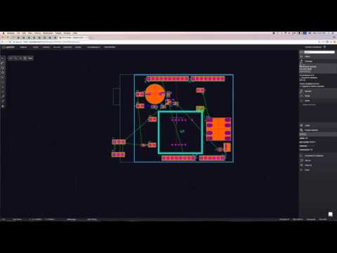
Let's make PCB design easier #sponsored by NextPCB

Показать описание
In this video I talk a bit about PCB fabrication and design, specifically using NextPCB's DFM software, a tool which helps you identify issues in your designs before you send them away for manufacturing. It's great for hobbiests just getting into PCB design and helpful to catch basic mistakes even for experts!
 0:01:00
Let's make PCB design easier #sponsored by NextPCB
 0:10:40
PCB Creation for Beginners - Start to finish tutorial in 10 minutes
 0:12:52
Top 5 Beginner PCB Design Mistakes (and how to fix them)
 1:09:57
Upverter // Making PCB Design Easy, Powerful and Approachable
 0:33:06
An Absolute Beginners Guide To Designing PCBs using Easy EDA - Make PCB From A Schematic Part 2
 0:00:42
Make a PCB with ChatGPT ! 🤖 #electronics #pcbdesign #altiumdesigner #kicad #pcb #fyp #jlcpcb
 0:00:13
Mastering PCB Design with Quick Route Fanout | Autodesk Fusion 360
 0:33:10
An Absolute Beginners Guide To Designing PCBs using Easy EDA - Make PCB From A Schematic
 0:11:05
Flawless PCB design: 3 simple rules - Part 2
 0:00:26
✨Let's Solder PCB Together! #jlcpcb #pcb #diy #maker #electronics #pcba #soldering #pcbdesign
 0:00:17
Designing PCBs doesn't have to be hard #pcb #circuitboard #electricalengineering
 0:01:00
Don't Need Dedicated Power Layer! 1 Minute #pcbdesign #designreview #electronics
 0:00:40
Running LED tower | LED circuits | Electronics projects
 0:19:36
Let's make a PCB using an online service for professional results! Tutorial
 0:00:13
PCB Prototyping Made Easy
 0:17:13
Learn PCB Designing Just in 15 Minutes! EasyEDA + JLCPCB Complete Tutorial 2023
 0:00:19
A Simple PCB Enclosure Design #385 #tutorial #designwithajay #SolidWorks #tutorial @DesignWithAjay
 0:01:00
Gorgeous PCB Layout! | 1-Min #PCBDesign
 0:18:49
How To Learn PCB Design (My Thoughts, Journey, and Resources) - Phil's Lab #87
 0:14:41
How to make your First PCB! Beginner KiCAD Design Tutorial
 0:10:44
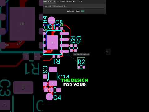
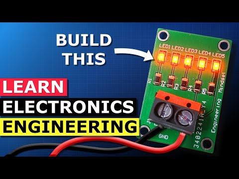
Design and Build a PCB - SMD LED Learn electronics engineering
 0:36:25
Tutorial - How to Design a PCB
 0:04:11
Quick and Simple PCB designing
 0:28:48
How to Design a PCB easily with EasyEDA - Complete Tutorial Series
Комментарии