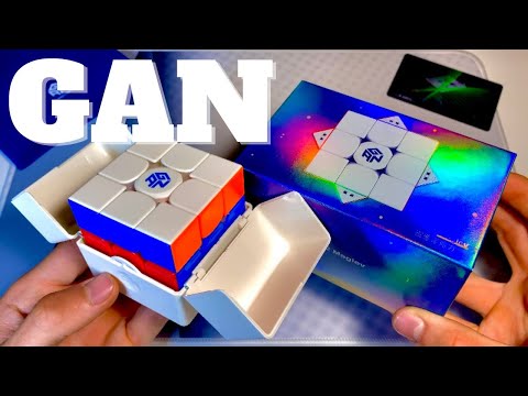
Should you buy a GaN Power Adapter? Or is it a scam? || Testing GaN FETs!

preview_player
Показать описание

In this video we will be having a closer look at GaN FETs in order to find out whether they will improve power electronics products in the future. For that I got myself a commercial GaN power adapter which I will compare with a more traditional power adapter concerning their efficiency. Afterwards I will measure the resistance and switching speed of a proper GaN FET and finally use it in a buck converter circuit to demonstrate the difference to a normal MOSFET. Let's get started!

Websites which were shown (used) during the video:

Thanks to the Keysight University Live for sponsoring this video.

Music:
2011 Lookalike by Bartlebeats

0:00 Introduction to GaN FETs (Power Adapters)
1:58 Intro
2:50 Testing the efficiency of a GaN Power Adapter and a traditional one
5:43 Selecting a proper GaN FET
6:08 Resistance Test (GaN FET VS MOSFET)
7:00 Switching Test (GaN FET VS MOSFET)
9:46 Buck Converter Test (GaN FET VS MOSFET)
10:42 Conclusion
Рекомендации по теме
Комментарии
Автор

So in short GAN is not a scam but the adapter that didn't have one in it is! :)

noanyobiseniss
Автор

GaN and Mosfet: _fighting_
Silicon Carbide: _Record the fight_
IGBT: _watching from far away_
Bjt: *in the corner*
Ujt: _buried in the grave_
Thyristor family: 👏👏 *impressive*
Vacuum tube: _in the hall of fame_

Arctic_silverstreak
Автор

I think what's more important to most consumers than minor savings on their electric bill is actually the simple fact that a GaN charger can be physically smaller than a traditional silicon based one of equivalent power output.

CJDavies
Автор

So, a few things to point out (I play with power electronics for a living. I have a PhD on the topic of series connecting normally on power devices to obtain self balanced high voltage power modules. I now work in China for a state sponsored power electronics research facility, particularly on consumer and data center GaN and SiC applications):

1. GaN FETs are not nearly as expensive as depicted from DigiKey/Mouser. Western distributors are known to add a lot of profit on hard to sell (niche) items like GaN/SiC transistors and FPGAs. The real cost of those things rated for a 65W adapter (130~180mR typ., 600~650V max.) in China is around $1 for Chinese parts (InnoScience, etc.) and $1.5 for Western parts (GaN Systems, etc.). A comparable state of the art Si device will cost you $0.5 for Chinese parts (Wayon WMZ26N65C4) and $1 for Western parts (Infineon IPL60R185C7).

2. Transphorm makes D-mode GaN, which is normally on. They have a reliability advantage due to the lack of atom-thin gate structure, so they are commonly used in automotive applications and military RF applications. For consumer stuff, E-mode is more commonly used due to it being normally off. To make a D-mode device normally off, you need to series connect a low voltage Si MOSFET, so when the MOSFET is off, the drain potential of the Si MOSFET (which is tied to the source of the GaN HEMT) is pulled high, since the gate of the GaN is tied to the source of the Si MOSFET, the GaN sees a negative voltage on its gate with respect to its source, so it turns off. So what you are measuring is actually the input characteristics of the Si MOSFET, not the GaN.

3. Gate charge determines how easily and efficiently the FET is driven, not how it outputs (for most high voltage applications, Qout is much more important than Qin due to much higher Vds than Vgs). For GaN, the output figure of merit number does not look good, even for E-mode devices. Only in very few applications like QR flyback GaN has a marginally advantage compared with Si, and even that is mostly for marketing reasons. For most applications, rest of being able to be driven faster and switch faster (which can be done equally well with well designed Si drivers, anyway you are limited by EMI regulations), they do not possess a much better performance compared with Si.


4. About reverse recovery, E-mode GaN does not have a reverse recovery charge, but they have horribly high Vf in third quadrant freewheeling mode, some 3V~4V. Cascade D-mode GaN does have a reverse recovery charge from the series connected Si MOSFET body diode. This can be alleviated by parallel connecting a low voltage Schottky diode with the MOSFET, but so far I've not seen this being done, probably for patent reasons. Cascade devices do have lower freewheeling Vf due to the GaN is in conduction mode (since there can't be a gate bias voltage from nowhere and they are normally on), the only Vf (other than Rdson*If) comes from the body diode of the Si MOSFET.

5. Some of the smallest and densest chargers are Si, like the Delta Innergie 60C. The biggest reason why GaN is massively used in chargers is because Xiaomi invested in a large portion of Navitas and Xiaomi wants Navitas to bloom, so Xiaomi used its consumer electronics market dominance to drive the market towards GaN. When other companies see this novelty marketing makes money, they so the same, that's what landed the market now what it is.


References:

1. My visits to suppliers.
2. Trahsphorm website, VisIC website.
3. Trahsphorm website, VisIC website and USCi website.
4. EPC, GaN Systems and Transphorm datasheets.
5. Innergie kickstarter page and some market research reports.
6. The website itself.

bskull
Автор

Your mid-air circuit has some sort of ElectroBOOM vibes to it, minus the explosions though.

Asu
Автор

GaN Fets are maybe not a scam but some Products wich say they offer GaN Fets :D Because they use traditional cheap mosfets and to increase their margin with the GaN selling point

ResurrectionofMC
Автор

Simply swapping a GaN FET into a given switching circuit will provide only modest gains; the main advantage is that you can then use a higher switching frequency without the gate charge becoming a limiting factor for efficiency, so you can reduce the size of your other components and by extension reduce losses in them too. You also covered both gate charge and on resistance independently, but the real benefit with a GaN is the ratio or relationship between these. You can easily get silicon MOSFETs with on resistances way lower than the one you looked at, but it would have a huge gate charge which increases losses elsewhere in the circuit. This relationship can be considered a "figure of merit" for comparing switching transistors, and it's simply much better in GaN fets at any size/rating.

In general, the end result is much *smaller* power adapters with slightly better efficiency; in practice the efficiency of a USB adapter really won't have a major impact on somebody's power bill (because USB devices are only a small fraction of somebody's total power bill), but having a smaller adapter for the same output is a definite advantage to most people!

As another aside, silicon carbide is also starting to be used in power applications (similar "figure of merit" improvements compared to silicon). Due to their characteristics, you'll usually see GaN used in lower power and lower voltage applications (like consumer power adapters) while SiC is often selected for higher voltage applications like inverters in electric cars.

siberx
Автор

"Stay creative....and I will see you next time!!!"

*Covers webcam just in case.

anotheruser
Автор

Nice video, Big advantages at GaN over fets is at high current applications such as inverters for auto/motor industry... You missed the point that the reason why they are used in domestic applications is that they allow for smaller inductors due to faster switching therefore miniaturisation...

eryksokolowski
Автор

One of the big selling points of GaN chargers as I understand it is also power density. Because we can switch faster, we can use smaller storage components in the DC side. This means that we can end up with a charging brick that is drastically smaller because the Caps can be way smaller.

SeaMushroom
Автор

I always find myself so in awe of your clear, square drawing skills <3

CalMariner
Автор

This is reminiscent of the "graphene" power banks. They just add a new buzzword as a sales gimmick.
I'm not sure I'm comfortable with the promise of hundreds of watts of power in tiny plug-top PSUs. The words "bang" and "skidmark" come to mind.

bigclivedotcom
Автор

I love the crossover between material sciences and electronics! Thank you for the video!

mydprintedlife
Автор

As a marketing guy (formerly in product development), I need to tell you that the vast majority of consumers want a low purchase price in combination with big brand name, giving them status amongst their peers. A smaller group wants good specs (on paper) - so they can justify the purchase. Only a small minority has the mental horsepower to separate important features from marketing fluff and eye candy and will base purchasing decisions on validated performance.

f.d.
Автор

GaN FETs are not a scam, but sure looks like that the "GaN" power adapter you bought is...

largepimping
Автор

It’s really awesome that the chargers are now much smaller at same power.
100w bricks aren’t that bulky anymore.
That’s the main difference that gan tech makes.

daniel__
Автор

It's newly discovered but amazed to find it these early in device

c.schandra
Автор

GaNs are definitely not a scam. With GaN, MHz converters are realized decreasing volume of power supplies. I worked on a 1.2kW Power supply with GaN HEMTs, we were able to achieve titanium efficiency because the GaN allowed us to use a bridgeless topology which would have been impossible with silicon FETs.

ahmedkotb
Автор

What I like about GaN the most is the size. Getting a 65w GaN charger is much smaller than a silicon one.

One company even makes a 20w GaN charger in the same space as Apple's old 5w charger.

christian
Автор

I think one of the main reasons why GaN is still expensive is that the wafer diameters are typically smaller than silicon wafers (4 or 6 inch vs 12 inch). However they have been increasing in recent years, so that that may reduce the cost eventually.

funtechu