filmov
tv
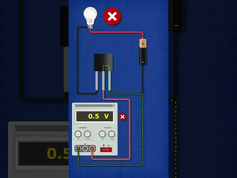
Transistor input and output Characteristics in tamil

Показать описание
Transistor input and output Characteristics
In this transistor tutorial, we will learn about Different Configurations of Transistors. Since a Bipolar Junction Transistor is a 3-terminal device, there are three different configurations of Transistors possible with BJTs. Understanding these different configurations of transistors will help you in better implementation of your application.
Introduction
We know that generally the transistor has three terminals – emitter (E), base (B) and collector. But in the circuit connections we need four terminals, two terminals for input and another two terminals for output. To overcome these problems we use one terminal as common for both input and output actions.
Using this property we construct the circuits and these structures are called transistor configurations. Generally there are three different configurations of transistors and they are common base (CB) configuration, common collector (CC) configuration and common emitter (CE) configuration.
The behavior of these three different configurations of transistors with respect to gain is given below.
1.Common Base (CB) Configuration: no current gain but voltage gain
2.Common Collector (CC) Configuration: current gain but no voltage gain
3.Common Emitter (CE) Configuration: current gain and voltage gain
Common Base Configuration.
In this configuration we use base as common terminal for both input and output signals. The configuration name itself indicates the common terminal. Here the input is applied between the base and emitter terminals and the corresponding output signal is taken between the base and collector terminals with the base terminal grounded. Here the input parameters are VEB and IE and the output parameters are VCB and IC. The input current flowing into the emitter terminal must be higher than the base current and collector current to operate the transistor, therefore the output collector current is less than the input emitter current.
The current gain is generally equal or less than to unity for this type of configuration. The input and output signals are in-phase in this configuration. The amplifier circuit configuration of this type is called as non-inverting amplifier circuit. The construction of this configuration circuit is difficult because this type has high voltage gain values.
The input characteristics of this configuration are looks like characteristics of illuminated photo diode while the output characteristics represents a forward biased diode. This transistor configuration has high output impedance and low input impedance. This type of configuration has high resistance gain i.e. ratio of output resistance to input resistance is high. The voltage gain for this configuration of circuit is given below.
AV = Vout/Vin = (IC*RL) / (IE*Rin)
Current gain in common base configuration is given as
α = Output current/Input current
α = IC/IE
The common base circuit is mainly used in single stage amplifier circuits, such as microphone pre amplifier or radio frequency amplifiers because of their high frequency response.
Input Characteristics
Input characteristics are obtained between input current and input voltage with constant output voltage. First keep the output voltage VCB constant and vary the input voltage VEB for different points then at each point record the input current IE value. Repeat the same process at different output voltage levels. Now with these values we need to plot the graph between IE and VEB parameters. The below figure show the input characteristics of common base configuration. The equation to calculate the input resistance Rin value is given below.
Rin = VEB / IE (when VCB is constant)
Output Characteristics
The output characteristics of common base configuration are obtained between output current and output voltage with constant input current. First keep the emitter current constant and vary the VCB value for different points, now record the IC values at each point. Repeat the same process at different IE values. Finally we need to draw the plot between VCB and IC at constant IE. The below figure show the output characteristics of common base configuration.
Thank You for watching
Комментарии
 0:13:12
 0:08:53
 0:07:21
 0:13:57
 0:11:44
 0:10:08
 0:10:23
 0:08:52
 0:48:43
 0:11:29
 0:06:31
 0:10:23
 0:13:57
 0:02:36
 0:14:41
 0:34:53
 0:07:47
 0:04:00
 0:00:16
 0:11:57
 0:05:23
 0:06:46
 0:01:00
 0:09:46