filmov
tv
Output characteristics of NPN transistor | Class 12 (India) | Physics | Khan Academy

Показать описание
Let's explore the behaviour of output current (collector current Ic) as the output voltage (Vce) is changed in an NPN transistor.
Class 12 Semiconductors: We cannot imagine our life without computers today. But what makes a computer tick? What's making this technology grow at such an exponential rate? It's all due to semiconductors. As unbelievable as that might sound, altering the properties of semiconductors allows us to build these computers. In this topic, we will explore the world of semiconductors. It's a journey from what semiconductors are all the way to creating building blocks of these computers.
Khan Academy is a nonprofit organization with the mission of providing a free, world-class education for anyone, anywhere. We offer quizzes, questions, instructional videos, and articles on a range of academic subjects, including math, biology, chemistry, physics, history, economics, finance, grammar, preschool learning, and more. We provide teachers with tools and data so they can help their students develop the skills, habits, and mindsets for success in school and beyond. Khan Academy has been translated into dozens of languages, and 15 million people around the globe learn on Khan Academy every month. As a 501(c)(3) nonprofit organization, we would love your help!
Created by Mahesh Shenoy
 0:08:53
Output characteristics of NPN transistor | Class 12 (India) | Physics | Khan Academy
 0:13:57
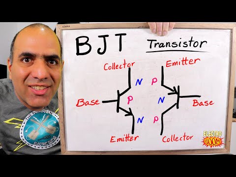
Starter Guide to BJT Transistors (ElectroBOOM101 - 011)
 0:07:21
Input characteristics of NPN transistor | Class 12 (India) | Physics | Khan Academy
 0:13:12
BJT: Common Emitter Configuration (Input and Output Characteristics) Explained
 0:08:58
Common emitter configuration
 0:09:27
BJT Characteristics
 0:24:23
transistor bjt input/output characteristics
 0:14:41
BJT : Common Base Configuration Explained
 0:03:38
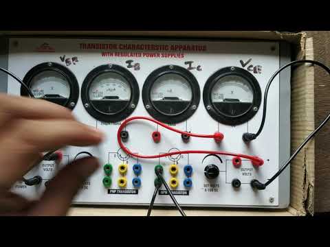
BJT Output Characteristics Simulation with Multisim
 0:10:23
Input and output characteristics of p-n-p common base transistor
 0:15:50
CE configuration Output Characteristics of NPN transistor
 0:05:14
NPN input output characteristics in CE configuration on proteus.
 0:07:15
Draw the typical input and output characteristics of an n-p-n trans...
 0:06:46
Common Emitter Transistor Configuration & Characteristics (in Bangla)
 0:00:16
Plot the input and output characteristics of given transistor in Common Base Configuration #shorts
 0:05:23
#24 common emitter configuration of a Transistor (BJT) || EC Academy
 0:14:09
ORCAD - Common Emitter Configuration: Input/Output Characteristics Curve of a Transistor (BJT)
 0:03:23
Simulation of Input and Output Characteristics of BJT in CE Configuration using MultiSim.
 0:04:16
NPN Transistor Common Emitter Experiment || V-I Characteristics
 0:07:47
Common Emitter Transistor Characteristics
 0:11:29
Input Output Characteristics of BJT | Electronic Devices and Circuits - 1 in EXTC Engineering
 0:11:44
#23 Common base configuration of a Transistor (BJT) | input & output characteristics || EC Acade...
 0:00:51
Characteristics of Common Emitter N-P-N transistor #hsc2022 imp question#shorts
 0:13:46
15 BJT Output Characteristics with Proteus Simulation
Комментарии