filmov
tv
Avalanche Breakdown: What is it?

Показать описание
Comment below with any additional questions you have. If you enjoyed this video and want to see more like it, please LIKE and SUBSCRIBE to our Youtube channel.
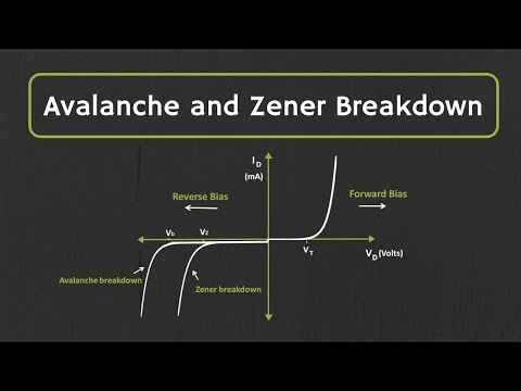
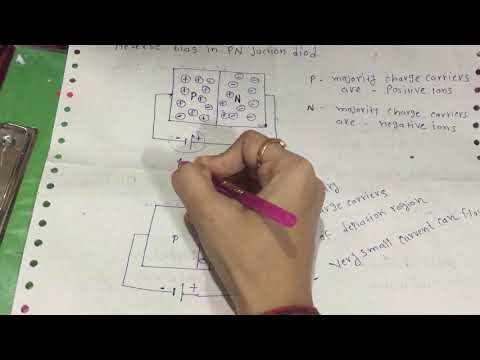
Avalanche breakdown (or “the avalance effect”) is a phenomenon that can occur in both insulating and semiconducting materials. It is a form of electric current multiplication that can allow very large currents within materials which are otherwise good insulators. It is a type of electron avalanche. The avalanche process occurs when carriers in the transition region are accelerated by the electric field to energies sufficient to create mobile or free electron-hole pairs via collisions with bound electrons.
There is a difference between Avalanche breakdown and Zener breakdown. In Zener breakdown, the electrons “tunnel” from the valence band of the p side to the conduction band on the n side. In classical physics, electrons should not have been able to cross over in this way. Tunnelling is, in fact, a quantum mechanical phenomenon, which comes about from electrons having wave properties.
The main differences between Zener and Avalanche Breakdown are:
1. Zener breakdown and avalanche breakdown are processes by which diodes begin to conduct significant currents, when they are subject to a high reverse voltage.
2. Zener breakdown occurs when the doping levels are high, and involves electrons tunnelling from the valence band of the p side to the conduction band on the n side.
3. Avalanche breakdown occurs when charge carriers which are accelerated by the electric field gain enough kinetic energy such that, when they collide with lattice atoms, they ionise the lattice atoms to produce electron-ion pairs. These pairs, in turn, cause further ionisations, leading to an “avalanche” effect.
 0:05:35
Avalanche Breakdown: What is it?
 0:10:03
Avalanche Breakdown and Zener Breakdown Effect Explained
 0:13:44
Avalanche Breakdown and Zener Breakdown Effect Explained
 0:03:05
Zener Breakdown: What is it?
 0:08:54
PN breakdown and avalanche | Class 12 (India) | Physics | Khan Academy
 0:06:14
Avalanche Breakdown
 0:00:52
How the Avalanches occur
 0:08:13
What is Avalanche breakdown ? MOSFET Avalanche breakdown
 0:00:36
An accidentally triggered snow slab avalanche
 0:13:21
Avalanche vs. Tunneling: how can you distinguish between the two breakdown mechanisms ?
 0:05:24
Avalanche Breakdown and Zener breakdown
 0:03:23
World's Biggest #Avalanche - 2 contrasting views
 0:00:59
difference between Zener and Avalanche Breakdown//@brevilearning
 0:12:45
Semiconductors L13: Zener Diode | Zener breakdown vs Avalanche Breakdown | Physics Endgame
 0:04:47
Breakdown Voltage Avalanche Breakdown Zener Breakdown - Digital Electronics - Basic Electronics
 0:12:45
Zener diode & Zener breakdown | Class 12 (India) | Physics | Khan Academy
 0:08:34
Difference between the Zener | Avalanche Breakdown
 0:00:43
What is Zener Effect and Avalanche Effect | Basic Electronics
 0:00:09
Avalanche breakdown!!!😳
 0:18:57
Zener Diode (Zener Diode as Voltage Regulator) Avalanch effect & Zener effect
 0:02:44
Avalanche breakdown
 0:00:46
How does Zener breakdown differ from Avalanche breakdown? #zenerdiode #avalanche #interview #shorts
 0:04:38
AVALANCHE BREAKDOWN VS ZENER BREAKDOWN| SEMICONDUCTOR DEVICES | PART NO 16
 0:08:15
avalanche breakdown | Zenor diode |
Комментарии