EEVblog #155 - ITead Studio PCB Prototype Goof

preview_player
Показать описание
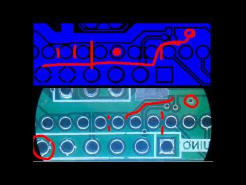
Dave shares an experience with his new prototype PCB's from ITead Studio.
Super awesomely cheap, but beware!
Рекомендации по теме
Комментарии
Автор

Dave, it looks like they changed the drill size, probably to reduce the amount of drill sizes. The bigger drill size made the pads a bit bigger and therefore the mask had to be changed resulting in a different spacing and the brake in the ground plane...

peterh
Автор

Actually PCB manufacturers do have a specification for minimum ring size around a drill, just so they can rule out issues because of misaligned drill (which does happen a lot with low cost fabs). So maybe they expanded the ring size and ended up causing issues. They should notify you - but it is good to take this into account in design phase.

mcuembedded
Автор

Even an error from iTead Studio is an opportunity for you to teach us something new, Thanks a lot for your effort Dave. Greetings from Mexico

jn
Автор

@Zadster Nope, they touched it. Otherwise why is that every single spacing around the ground plane is pulled back an exact distance, yet 6 thou tracks and spaces elsewhere on the board are perfectly intact? Etchent is not selective! The only explanation is they fiddled with the gerbers.

EEVblog
Автор

I've had companies use a different drills. I now look at the standard drills. Maybe they expanded the annular ring since you had very little copper.

jeriellsworth
Автор

I'm studying Electrical Engineering, and I just want to thank you Dave, as I've learned so much from your videos! And it's nice that you come with hints like this, you don't learn stuff like that on uni.

zarserz
Автор

@BarriosGroupie I am not to blame in any way, nor was it bad design practice. Those ground traces between pads were 8thou wide!

EEVblog
Автор

@yanava Ouch, how did that happen? Extra traces added? Bizarre.

EEVblog
Автор

@mindthomas grounded scopes can be handy because you often don't have to bother with the ground clip lead just to view a simple non-critical signal. But when you need an isolated scope, there is no substitute.

EEVblog
Автор

@flamzart I have never had this issue with any other manufacturer, ever. So I don't think anyone should be expected to change their process just for ITead.

EEVblog
Автор

@CampKohler I did, and it works a treat. Well, entire board not fully tested yet, need more firmware for that...

EEVblog
Автор

@EEVblog Yep, there were some extra traces. It shorted two terminals from a 25MHz crystal to ground. As a result, a network chip attached to it would respond to some commands and not to others. After wasting an arm an a leg calling the chip manufacturer I ended up looking at the board and found the short circuits. I don't know if you already done a blog on "putting a pcb to work" but it would be an excellent idea to show basic validation steps for a PCB.

yanava
Автор

@jeriellsworth Annular rings look the same size, so that doesn't look like the explanation. A good board house should have all drills in small enough increments. And they drill smaller and then plate out to the required size anyway.

EEVblog
Автор

Not all notebooks are isolated (some with a three-prong earthed pack; obviously unearthed packs are isolated). Mine has a power pack with a path from earth to the DC ground, and that actually causes audio ground loop issues because there's a high-current ground path over a crappy DC cable which makes it drop some voltage. So whenever I hook up any audio device that's also grounded I get an annoying buzz. I mostly fixed it by adding a nice fat ground from a connector shield to mains earth.

marcan
Автор

I try to make sure a circuit is electrically sound before pouring the copper planes. In altium you can "shelve" the polygons, then do the DRC. This method makes sure I have explicit traces that follow DRC width rules for every pwr and gnd pin.
On the other hand, my boss and others rely on poured polygons to complete their circuit.

cucheshire
Автор

I have had a dozen or so PCBs from itead studio. All were great. But I use 8 thou design rules.

FPVSlacker
Автор

Nice Vid Dave. Our PCB maker actually some "little" changes on the PCB's. Sometimes adds some test points to make internal tests like continuty between tracks. Sometimes they just can solve the resolution, change track witdh or clerance.
Related to the ground, you mentioned that the board is actually high density to route a ground track. What try to I do is to route ground, run DRC without any fill planes and once iI've get 0 errors, I feel deligthfull on filling the PCB with ground fills =)

bytefree
Автор

Thanks for the detailed troubleshooting of your problem; that kind of experience is good for a student like me.

errold
Автор

And please keep up those explanations for those of us still learning. Thanks Dave for the explanation.

BadQuantum
Автор

@frank26080115 Sometime you are forced to use design minimums like in this case. What do you do then?

EEVblog