filmov
tv
EEVblog 1415 - Reverse Engineering the DP10007 Differential Probe

Показать описание
Reverse engineering the Micsig DP10007 high voltage differential probe.
Turning the PCB into a schematic.
Buy anything through that link and Dave gets a commission at no cost to you.
Donate With Bitcoin & Other Crypto Currencies!
#ElectronicsCreators #HowTo #ReverseEngineering
Turning the PCB into a schematic.
Buy anything through that link and Dave gets a commission at no cost to you.
Donate With Bitcoin & Other Crypto Currencies!
#ElectronicsCreators #HowTo #ReverseEngineering
 0:29:00
EEVblog 1415 - Reverse Engineering the DP10007 Differential Probe
 0:38:58
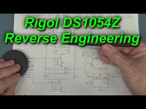
EEVblog #675 - How To Reverse Engineer A Rigol DS1054Z
 0:29:07
EEVblog 1521 - CMRR Full Edit
 0:15:58
EEVblog 1414 - MicSig DP10007 High Voltage Probe - Turning it up to 11
 0:13:17
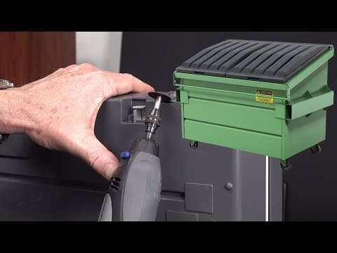
EEVblog 1421 - Epson Dumpster Hack
 0:11:33
eevBLAB 88 - Right To Repair Questions & Answers
 0:16:43
CMRR Followup Micsig DP10007 vs HVP70
 0:29:23
EEVblog 1416 - Random TEARDOWN: Sennheiser EW100 True Diversity Receiver
 0:27:06
EEVblog 1407 - Right to Repair with iFixit Founder Kyle Wiens
 0:19:57
EEVblog 1511 - Solar Analytics System FAIL! (+ Dave gets ZAPPED!)
 0:26:57
EEVblog 1423 - Flaming Magic Repair Smoke!
 0:38:46
EEVblog 1413 - Oscilloscope Current Probe TEARDOWN + DEMO
 0:30:43
EEVblog #1032 Part 5 - John Kenny Keysight Interview
 0:19:56
EEVblog 1521 - Common Mode Rejection Ratio (CMRR) Explained & Measured
 0:24:47
Ultralow Noise Tester: 9V Battery vs. 7805 vs. LTZ1000
 0:00:57
Lab Oil Spill!
 0:29:58
EEVblog #1367 - 5 Types of Oscilloscope Passive Probes COMPARED
 0:01:59
My First Paid Electronics Gig
 0:01:57
EEVblog #560 - How To Remove Sticker Residue On Test Equipment
 0:21:02
Open Source IC Design and Hardware Reverse Engineering Or: How I Learned to Stop... Johanna Baehr
 0:15:03
Evaluating the test results of a 5000:1 HV probe
 0:02:40
Interesting Dumpster Find
 0:11:43
EEVblog #1303 - New Lab LED Panels
 0:15:12
2.5Ghz Active Probe HP Agilent Keysight 1152A probe 5V Conversion Patch
Комментарии