filmov
tv
Introduction to FPGA Part 3 - Getting Started with Verilog | Digi-Key Electronics

Показать описание
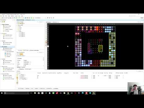
In this tutorial, we demonstrate how to use continuous assignment statements in Verilog to construct digital logic circuits on an FPGA.
A field-programmable gate array (FPGA) is an integrated circuit (IC) that lets you implement custom digital circuits. You can use an FPGA to create optimized digital logic for things like digital signal processing (DSP), machine learning, and cryptocurrency mining. Because of the FPGA’s flexibility, you can often implement entire processors using its digital logic. You can find FPGAs in consumer electronics, satellites, and in servers used to perform specialized calculations.
In this series, we will see how an FPGA works and demonstrate how to create custom digital logic using the Verilog hardware description language (HDL).
We start by showing how to define pins using a physical constraints file (.pcf), which maps Verilog I/O signal names to physical pin numbers on the FPGA package. Refer to the following documents to see the pinout on the iCE40HX1K and how it’s connected on the iCEstick:
- iCE40 LP/HX Datasheet
- iCEstick Evaluation Kit User’s Guide
From there, we show how lookup tables are used to construct digital circuits inside the FPGA. We design a very simple digital circuit (a simple AND gate with pushbutton inputs) in Verilog, synthesize it, and upload it to the iCEstick.
Next, we demonstrate how vectors work in Verilog (as a bus of wires) and how to branch wires using the replication operation.
Your challenge is to create a 1-bit full adder as shown in this Wikipedia article.
Product Links:
Related Videos:
Related Project Links:
Related Articles:
Learn more:
Комментарии
 0:20:44
 0:59:24
 0:05:23
 0:01:26
 0:08:49
 0:07:27
 0:43:06
 0:36:47
 0:15:21
 0:16:24
 0:13:29
 0:23:17
 0:18:09
 0:21:22
 0:24:24
 0:13:26
 1:13:00
 0:05:00
 0:34:57
 0:04:49
 0:41:02
 0:06:22
 0:40:19
 0:28:31