filmov
tv
Introduction to FPGA Part 4 - Clocks and Procedural Assignments | Digi-Key Electronics

Показать описание
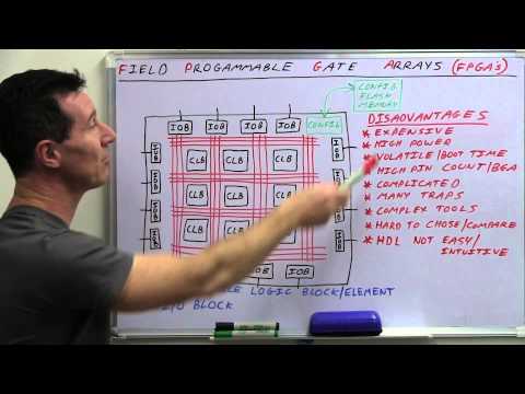
A field-programmable gate array (FPGA) is an integrated circuit (IC) that lets you implement custom digital circuits. You can use an FPGA to create optimized digital logic for things like digital signal processing (DSP), machine learning, and cryptocurrency mining. Because of the FPGA’s flexibility, you can often implement entire processors using its digital logic. You can find FPGAs in consumer electronics, satellites, and in servers used to perform specialized calculations.
In this series, we will see how an FPGA works and demonstrate how to create custom digital logic using the Verilog hardware description language (HDL).
We start by showing how the D flip-flop in an FPGA logic cell can be used to store a 1-bit value for one or (potentially) more clock cycles. Multiple D flip-flops can be combined with combinational logic gates to create hardware circuits that operate sequentially. We can control this sequential logic through Verilog blocks known as “procedural assignment statements.”
Next, we demonstrate a procedural assignment statement by constructing a simple 4-bit counter inside of an “always block.” Each time a button is pressed, the value increments by 1. The counter value is shown on the LEDs (in binary).
Note that you will likely experience button bounce that we have not accounted for in the demonstration. As a result, the counter will likely skip values each button press. You would need to implement button debounce circuitry (either in hardware or in HDL) to correct for this behavior. We will cover button debounce in a future episode.
Your challenge is to create a clock divider for the onboard 12 MHz oscillator (assuming you are using the iCEstick, the 12 MHz oscillator is connected to pin 21). The clock should be divided to 1 Hz, and this new clock signal should run the counter shown in the video. The new counter should increment on its own once per second.
Product Links:
Related Videos:
Related Project Links:
Related Articles:
Learn more:
 0:18:09
Introduction to FPGA Part 4 - Clocks and Procedural Assignments | Digi-Key Electronics
 0:24:24
Introduction to FPGA Part 5 - Finite State Machines | Digi-Key Electronics
 0:20:44
Introduction to FPGA Part 3 - Getting Started with Verilog | Digi-Key Electronics
 0:11:01
First Project With Lattice FPGA - Part 4: Simulation
 0:15:21
Introduction to FPGA Part 1 - What is an FPGA? | Digi-Key Electronics
 0:11:51
4. Xilinx Large FPGAs - Introduction to FPGA Design for Embedded Systems
 0:34:11
Introduction to FPGA's and VHDL - Part 4 GHDL Setup and Development Workflow
 0:12:31
Building a CPU on an FPGA, part 4
 2:17:01
Introductory Session: Fundamentals of Digital System Design 2024
 0:01:26
What's an FPGA?
 0:04:44
Intro to FPGAs for Software Engineers - Part 4 - Hello World Project (Part II)
 0:08:46
4. LUTs and FPGA Architecture - Introduction to FPGA Design for Embedded Systems
 0:16:35
Introduction to FPGA Part 6 - Verilog Modules and Parameters | Digi-Key Electronics
 0:00:34
Senior Programmers vs Junior Developers #shorts
 0:05:42
FPGA Design with MATLAB, Part 4: Converting to Fixed Point
 0:27:03
Introduction to FPGA Part 7 - Verilog Testbenches and Simulation | Digi-Key Electronics
 0:18:51
Introduction to FPGA Part 2 - Getting Started with Yosys, IceStorm, and Apio | Digi-Key Electronics
 0:37:44
EEVblog #496 - What Is An FPGA?
 0:17:36
Getting Started with FPGA Design #4: Embedded C Application Basics in FPGAs
 0:04:59
Vision Processing for FPGA, Part 4: Targeting a Lane Detection Design to a Xilinx Zynq Device
 0:23:06
Introduction to FPGA Part 11 - RISC-V Softcore Processor | Digi-Key Electronics
 0:22:34
Gigabit Ethernet + FPGA/SoC Bring-Up (Zynq Part 4) - Phil's Lab #99
 0:36:06
Getting Started with Microsemi SmartFusion2 System on Chip (Part 4) – FPGA Fabric Demonstration
 0:12:28
Getting started with the Lattice iCE40 FPGA: Programming w/ Open Source Tools (Part 4)
Комментарии