filmov
tv
Wave Soldering Process

Показать описание
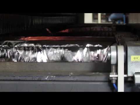
Wave soldering is a bulk soldering process used for the manufacturing of printed circuit boards. The circuit board is passed over a pan of molten solder in which a pump produces an upwelling of solder that looks like a standing wave.
Wave soldering is a common method used in PCB assembly to solder through-hole electronic components onto a printed circuit board (PCB). Here's an overview of the wave soldering process:
1 Preparation: Before wave soldering can begin, the PCB is prepared by applying solder paste to the through-hole component leads or by placing solder preforms in the holes.
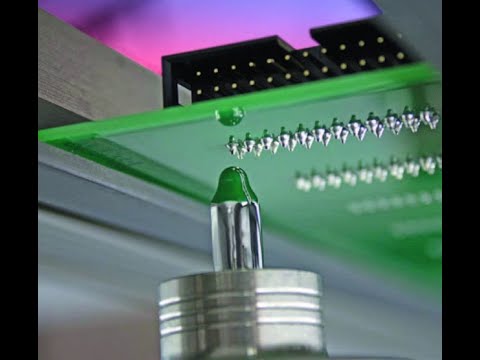
2 Flux Application: Flux is applied to the areas of the PCB where soldering will occur. Flux helps clean the metal surfaces, removes oxides, and promotes wetting, ensuring good solder connections.
3 Component Insertion: Electronic components with leads are inserted into the appropriate holes on the PCB. The components are held in place either by hand or by using fixtures.
4 Preheating: The PCB is preheated to a temperature below the melting point of the solder. Preheating helps to reduce thermal shock to the components during soldering and ensures uniform heating across the PCB.
5 Wave Soldering: The PCB is passed over a wave of molten solder. The solder wave is typically made of a mixture of tin and lead (though lead-free solder is also used for environmental reasons). As the PCB passes over the wave, the solder adheres to the exposed metal surfaces, forming solder joints between the component leads and the PCB pads.
6 Cooling and Solidification: After passing through the solder wave, the PCB moves to a cooling zone where the solder solidifies, forming strong electrical connections between the components and the PCB.
7 Cleaning: Once the solder has cooled, the PCB may be cleaned to remove any flux residues or other contaminants. This can be done using various methods such as water washing, solvent cleaning, or vapor degreasing.
8 wave soldering temperatureInspection: The soldered PCB is inspected to ensure that all components are properly soldered and that there are no defects or solder bridges.
Wave soldering is a common method used in PCB assembly to solder through-hole electronic components onto a printed circuit board (PCB). Here's an overview of the wave soldering process:
1 Preparation: Before wave soldering can begin, the PCB is prepared by applying solder paste to the through-hole component leads or by placing solder preforms in the holes.
2 Flux Application: Flux is applied to the areas of the PCB where soldering will occur. Flux helps clean the metal surfaces, removes oxides, and promotes wetting, ensuring good solder connections.
3 Component Insertion: Electronic components with leads are inserted into the appropriate holes on the PCB. The components are held in place either by hand or by using fixtures.
4 Preheating: The PCB is preheated to a temperature below the melting point of the solder. Preheating helps to reduce thermal shock to the components during soldering and ensures uniform heating across the PCB.
5 Wave Soldering: The PCB is passed over a wave of molten solder. The solder wave is typically made of a mixture of tin and lead (though lead-free solder is also used for environmental reasons). As the PCB passes over the wave, the solder adheres to the exposed metal surfaces, forming solder joints between the component leads and the PCB pads.
6 Cooling and Solidification: After passing through the solder wave, the PCB moves to a cooling zone where the solder solidifies, forming strong electrical connections between the components and the PCB.
7 Cleaning: Once the solder has cooled, the PCB may be cleaned to remove any flux residues or other contaminants. This can be done using various methods such as water washing, solvent cleaning, or vapor degreasing.
8 wave soldering temperatureInspection: The soldered PCB is inspected to ensure that all components are properly soldered and that there are no defects or solder bridges.
 0:02:19
Agrowtek Wave Soldering Process for Electronics Manufacturing
 0:00:39
Wave Soldering--PCB Assembly Process
 0:02:35
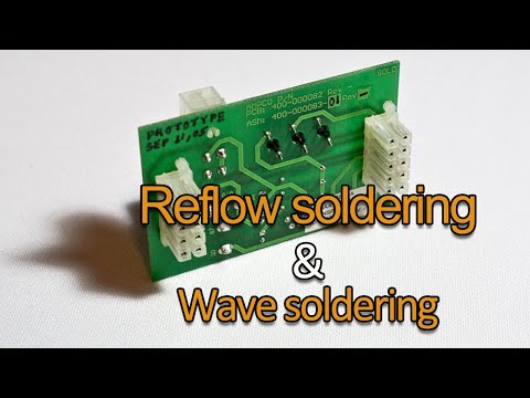
Reflow soldering and wave soldering【PCBBUY Protect】
 0:00:39
Wave Soldering Process
 0:03:40
Reflow, wave and hand soldering
 0:01:21
Wave Soldering Process Solutions from KIC
 0:00:14
Wave Soldering Process
 0:01:50
How does Wave Soldering Mastery work in PCBA
 0:00:39
DIP soldering process | Industrial Wave soldering
 0:02:24
WAVE SOLDERING PROCESS
 0:01:59
Wave Soldering Process for Electronics Manufacturing. PCB Through-Hole Assembly
 0:00:29
Reflow of Chip Component
 0:00:16
Wave Soldering
 0:04:21
How to Use Wave Soldering Equipment
 0:06:45
EEVblog #431 - PCB Wave Soldering
 0:00:45
Wave Soldering Process
 0:01:29
How the wave soldering machine works?
 0:00:48
YX250-Min Semi Auto Wave Solder Machine
 0:01:37
Wave Soldering Process & Machine Video Coming Soon.
 0:17:50
Wave Soldering Machine & Process, Types of Fluxing, Types of Preheater, Types of soldering wave.
 0:00:19
Wave Soldering Process for PCB Electronics Manufacturing. 【Consult Us Today】#electronics #pcb #smt...
 0:01:21
Wave soldering process introduction
 0:00:17
Selective Soldering, PCB Soldering.
 0:02:23
Wave soldering process | SMD THT PCB
Комментарии