filmov
tv
LED - Light Emitting Diode | Basics, Characteristics, Working & Applications | LED Vs PN Diode

Показать описание
Light Emitting Diode - LED is covered with the following outlines.
0. LED - Light Emitting Diode
1. Basics of LED
2. Symbol of LED
3. Internal Structure of Light Emitting Diode
5. Characteristics of Light Emitting Diode
6. Comparison of Light Emitting Diode and PN junction diode
7. Working of Light Emitting Diode
8. Applications of Light Emitting Diode
Chapter-wise detailed Syllabus of the Optical Fiber Communication Course is as follows:
Historical development of optical fiber communication (1G, 2G, 3G, 4G & 5G), Need of fiber optic communication system, Comparison of fiber optic communication system with copper wire communication system, Block diagram and working of fiber optic communication system.
Basics & structure of optical fibers, comparison of step index optical fiber and graded index optical fiber, single mode optical fiber and multi mode optical fiber, Comparison of Multimode step index fiber and Multimode graded index fiber, Refractive index of fiber, Refraction and Reflection of ray, Total internal reflection & critical angle, Snell's Law, Optical Fiber mode theory, Acceptance angle and Numerical Aperture, Normalized frequency, Relationship in between a number of modes and normalized frequency, acceptance angle & critical angle, Ray Optics representation.
Optical Fiber Fabrication, OVPO, VAD, MCVD, PCVD, Photonic Crystal Fiber PCF, Double Crucible Method, Fiber Materials.
Windows and spectral bands, Digital Transmission Hierarchy, Phase velocity and Group velocity in optical fiber, History of Attenuation in optical communication, Attenuation of signal, Material Absorption in optical fiber cable, Fiber Bending Losses, Scattering Losses in Optical fiber cable, Dispersion Losses in Optical fiber.
LED - Light Emitting Diode, Parameters of LED (Characteristics of LED, Quantum Efficiency of LED, Protection of LED, Effect of temperature & Irradiance of LED), LED Structure, Planar LED, Surface Emitting LED, Edge Emitting LED, Examples on LED, Comparison of LED and LASER, LASER, Mode Hopping of LASER, Frequency Chirps of LASER, Fabry Parot LASER, Distributed feedback LASER, Power Launched by LED in Step index Fiber, Power Launched by LED in Graded Index Fiber.
Lensing schemes of optical fiber, Fiber to fiber joint losses, Fiber Splicing, Optical fiber connectors, and Equilibrium Numerical Aperture.
Photo Diode, Figure of Merits of Photodiode (Quantum efficiency of Photodiode, Responsivity of Photodiode & Dark Current of Photo Diode), PIN Photodiode, Avalanche Photodiode, Comparison of PIN Photodiode & Avalanche Photodiode, Eye Diagram, Receiver Performance.
Point to point link of optical fiber communication system, Link power budget analysis of optical fiber system, Link power budget analysis, Rise time budget analysis.
Optical Amplifier, Semiconductor Optical Amplifier, EDFA - Erbium Doped Fiber Amplifier, Raman Amplifier.
Optical Couplers, Parameters of optical couplers (Optical splitting, Excess loss, Insertion loss & cross talk), Optical Isolator, Optical Circulator, OADM - Optical Add Drop Multiplexer.
WDM, DWDM, SONET/SDH.
OTDR, Dispersion Measurement, Eye Diagram.
Engineering Funda channel is all about Engineering and Technology. This video is a part of Optical Fiber Communication and Optical Communication.
#LED #OpticalCommunication #OpticalFiberCommunication @EngineeringFunda
 0:08:37
How LED works ⚡ What is a LED (Light Emitting Diode)
 0:10:27
LEDs - Light Emitting Diodes - Basic Introduction
 0:19:06
How LED Works - Unravel the Mysteries of How LEDs Work!
 0:04:15
How does an LED work at the molecular AND practical level? | Intermediate Electronics
 0:06:53
Light Emitting Diode (LED) Working Principle
 0:03:53
What is LED Light Emitting Diode | How Does LED Works | Electronic Devices & Circuits | Engineer...
 0:04:06
How does a Light Emitting Diode or LED work?
 0:07:47
LED working & advantages | Semiconductors | Physics | Khan Academy
 0:01:00
TEASER: Xiaomi Flexible Rechargeable Lamp
 0:10:20
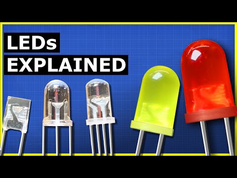
Light Emitting Diode (LED) Explained (Working, Advantages and Types of LED Explained)
 0:33:45
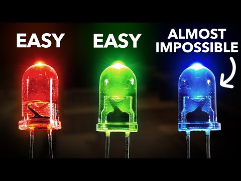
Why It Was Almost Impossible to Make the Blue LED
 0:04:56
LED Basics
 0:05:58
How do LEDs work? | LEDs Explained SIMPLE | What is a Light Emitting Diode? Electrical Science STEM
 0:17:00
How to Turn an LED On
 0:12:31
How to wire up and use LEDs (explained for beginners)
 0:10:56
LED - Light Emitting Diode | Basics, Characteristics, Working & Applications | LED Vs PN Diode
 0:05:36
Why all solar panels are secretly LEDs (and all LEDs are secretly solar panels)
 0:20:16
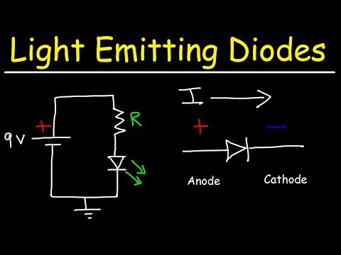
How to Calculate the Correct Resistor for LEDs Light Emitting Diodes
 0:14:12
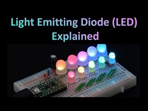
Building DIY LED lights
 0:05:13
History of LED Lights (light emitting diodes) | Basic Electronics
 0:03:40
LED Bulb, SMD LED Lights Testing and Checking With a Digital Multimeter || Light Emitting Diode ||
 0:04:51
How LED (Light Emitting Diode) Works? [3D Animation]
 0:11:06
My Collection of LEDs | Different Types of LED | Light Emitting Diodes | My LED Inventory in English
 0:00:11
LED is an efficient energy-saving light source, light-emitting diode, universal model
Комментарии