filmov
tv
Review of a PCB Layout: Do you do same mistakes? - For Beginners (Part 1 of 4)

Показать описание
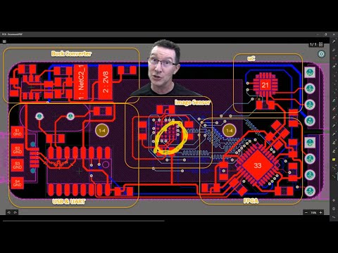
In this video series I am commenting a PCB layout done by someone starting with hardware design. We will speak about the things which could be done differently or which could be improved.
Would you like to support me in what I do? It's simple:
The other ways to support me in what I do are:
- send me an email and/or leave a positive comment
- watch and like the videos :)
- spread a word about FEDEVEL Academy
It is much appreciated. Thank you,
- Robert
Would you like to support me in what I do? It's simple:
The other ways to support me in what I do are:
- send me an email and/or leave a positive comment
- watch and like the videos :)
- spread a word about FEDEVEL Academy
It is much appreciated. Thank you,
- Robert
 0:15:11
Review of a PCB Layout: Do you do same mistakes? - For Beginners (Part 1 of 4)
 0:37:29
EEVblog #1323 - PCB Layout Review & Analysis
 0:24:29
Which PCB Design Software is The Best? The Top 4 Are ...
 0:00:59
Best and Worst PCB Design Software
 0:17:53
PCB Design Review Deep Dive
 0:18:16
Review of Server PCB Layout & Schematic - Part 1: Processor
 0:12:52
Top 5 Beginner PCB Design Mistakes (and how to fix them)
 0:16:12
Design Review - Schematic & PCB - Phil's Lab #70
 0:10:01
My New Workplace Custom Keyboard Featuring Monsgeek M3W and Akko Silent Penguin Tactile (Review)
 0:18:25
Review of Server PCB Layout & Schematic - Part 7: MISC
 0:05:51
PCB Design For Beginners: Ugly Tracks Are Noisy
 0:18:49
How To Learn PCB Design (My Thoughts, Journey, and Resources) - Phil's Lab #87
 0:10:40
6 Horribly Common PCB Design Mistakes
 0:05:27
How Do PCBs Work?
 0:12:49
Review of a PCB Layout: Do you do same mistakes? - For Beginners (Part 2 of 4)
 0:01:00
Yeah...That's an EMC Risk | 1 Min PCB Design Review
 0:19:58
Review of a PCB Layout: Do you do same mistakes? (Part 4 of 4)
 0:14:30
Review of Server PCB Layout & Schematic - Part 4: PCI Express (PCIE)
 0:01:00
Super Pro ESP32 RF PCB Layout: One Minute #PCBDesign Review 05 #electronics #altium
 0:08:10
EasyEDA Review - Online PCB design and PCB Manufacturing
 0:43:41
How To Improve Your PCB Layout - Power Planes
 0:01:56
High-Speed PCB Design Overview | Allegro PCB Designer
 0:29:52
USB-C Power Delivery Hardware Design - Phil's Lab #104
 0:27:53
Review of Server PCB Layout & Schematic - Part 6: DDR4 Memory Layout & CPU Power
Комментарии