filmov
tv
How to write SPI Interface code in Verilog HDL for a 12-bit ADC (using the DE0-Nano)

Показать описание
Writing SPI interface code for ADCs is all about getting the timing right. In this video, I go through, step by step, my process for writing SPI interface code in Verilog. I'm using the DE0-Nano FPGA development board with its on-board ADC128S022 - a 12-bit, 8-channel 200 ksps ADC. This video also serves as a good tutorial on the use of Signaltap for debugging FPGA signals in real time.
00:00- Introduction
00:49 - SPI Overview
2:38 - Looking at the datasheet for the ADC128S022
7:43 - Verilog code
14:21 - Simulation
26:19 - BDF development and programming the device
00:00- Introduction
00:49 - SPI Overview
2:38 - Looking at the datasheet for the ADC128S022
7:43 - Verilog code
14:21 - Simulation
26:19 - BDF development and programming the device
 0:11:50
Understanding SPI
 0:08:06
Basics of SPI communication | Different modes of SPI communication
 0:33:00
SPI: The serial peripheral interface
 0:53:43
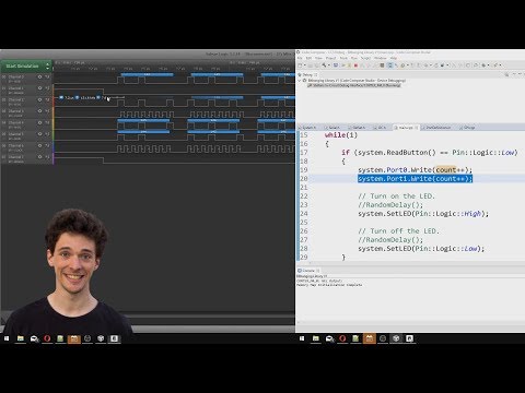
How to write SPI Interface code in Verilog HDL for a 12-bit ADC (using the DE0-Nano)
 0:10:31
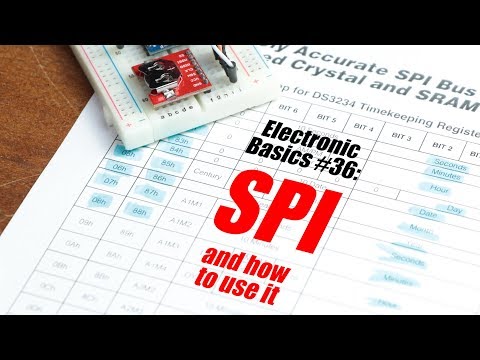
Electronic Basics #36: SPI and how to use it
 0:19:30
Getting Started with STM32 and Nucleo Part 5: How to Use SPI | Digi-Key Electronics
 0:17:42
Serial Peripheral Interface (SPI) Basics
 0:11:26
SPI Protocol Explained: Basics, Working, Modes, Pros and Cons
 0:08:07
'Analyzing Drought & Vegetation with SPI and NDVI in Google Earth Engine | Step-by-Step Tut...
 0:07:23
SPI communication Data Transmission | SPI communication Daisy chain
 0:17:34
EEVacademy #3 - Bit Banging & SPI Tutorial
 0:27:32
How To Write An STM32 SPI Driver (Full-Duplex Master Mode)
 0:05:07
Read/Write SPI and other serial interfaces from a PC
 0:08:19
Arduino Workshop - Chapter 5 - Using SPI
 0:14:30
Beginners Guide to SPI on the Raspberry Pi Pico (BMP280 Example)
 0:13:04
What is SPI? Basics for beginners!
 0:00:59
What is SPI Communication Protocol ? #ُembeddedsystem #embeddedsoftware #electronics
 0:00:14
🔥Watch the concept : How I2C, SPI, UART communication works ? #vlsi #chipdesign
 0:15:48
Tutorial 08 for Arduino: SPI Interfaces
 0:15:51
SPI communication basics (modes)
![[ES-EN-40] SPI PROTOCOL](https://i.ytimg.com/vi/iNRfumxqyI8/hqdefault.jpg) 0:43:36
0:43:36
[ES-EN-40] SPI PROTOCOL WITH EXAMPLE || Embedded Systems
 0:04:36
Read & Write SPI and other serial interfaces from PC
 0:11:58
PROTOCOLS: UART - I2C - SPI - Serial communications #001
 0:10:56
STM32 Nucleo - Keil 5 IDE with CubeMX: Tutorial 6 - SPI Interface
Комментарии