Battery Charger & Protection & Boost 5V or 12V
preview_player
Показать описание

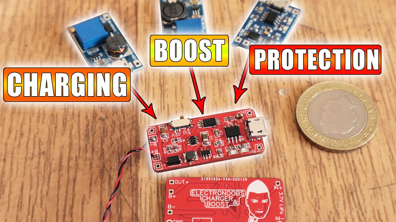
🔥I always use a 3.7V battery charger module and then I add a boost converter to get the 5V for my Arduino and so on. I wanted to have everything on the same PCB so I've used the protection ICs, charging and boost ICs and like that I have all I want on the same PCB. Hope you like it.

🔀LINKS
-------------------------------------

📺VIDEOS
-------------------------------------

🔬PRINTERS FDM
-------------------------------------
→ Coupon (324€) "D4FF9E1BE8227001"
→ Coupon (241€) "H4FF9DA22F227000"
→ Coupon (157€) "F4FE9A937B5EB000"
→ Coupon (157€) "J4FE99F73D5EB001"

🔅PRINTERS RESIN
-------------------------------------

Like share and subscribe to motivate me. Thank you

#PCB
#charger
#boost
Рекомендации по теме
Комментарии
Автор

12:04 To fix this issue just connect the 20K resistor permanently to the circuit. Then, just calculate which resistor value you need to put in parallel to that to make 7K, and just make the switch connect it in parallel. That way, you can either have 20K or 20K in parallel with whatever is connected to the switch. This means you'll never have a floating pin.

IscleGaming
Автор

Hi. It's a great idea, but I suggest two things to improve the circuit. First, use a FS312 instead of the DW01, because this chip have a 2.9V under voltage protection, instead of 2.5V, it's more safer for the Li-Po than the DW01. Second, use the switch to conmutate the R2 value, not the R1, in this configuration the FB pin always see the voltage of the output, and if the R2 value is floating, the voltage in the output will be 0.6V, the feedback reference voltage, and the IC is safe 👌🏻(Perdón si mi inglés no es muy bueno, pero prefiero comentar en inglés en tu canal de habla inglesa).

mundo_electronica
Автор

Cool board, but i guess i have a better solution to your problem. I suggest connecting the 20k ohm resistor (R1) permanently to the voltage divider so you would have 12V output and connect another resistor through a switch in parallel to the 20k resistor to obtain 5 volts output. This way the boost IC will always have its feedback loop closed.

dominikworkshop
Автор

Your channel really has become a wonderful source for electronics projects and building instructions for "finished parts" like this one. Thank you!

AngeEinstein
Автор

FANTASTIC. I've wished for such a circuit many times, to incorporate into my other PCB designs. I was too intimidated to try making my own so instead end up making headers on my PCB and piggybacking multiple modules. Since you did such an amazing job explaining this, maybe I can try to replicate it next time :-)

makermatrix
Автор

Also, be aware of the current rating on the surface mount switches. Good engineering design calls for at least 2x margin, i.e. if the battery can sustain ~500 mA the switch needs to handle *at least* 1000 mA. (This margin should be much higher than 2x if we were dealing with higher power.)

One solution is to use an N-channel mosfet to switch ground back to the battery. Then attach the smd switch to the gate to turn the mosfet on and off. But when it comes to things like power supply, I don't like low-side switching as it leaves the load energized, so if it finds a ground it might turn itself on.

So if you can find a p-channel mosfet that handles the required current and can be saturated at zero volts (rather than having to go negative) you can switch the high side of the battery instead. So look for a P-channel mosfet whose Vgs(th) is only about half of the voltage you want to switch. This increases the likelihood of the mosfet going into saturation.

Nono-hkis
Автор

I ordered some PCBs of the newer version. The components just came in. I can't believe you hand soldered this, the components are way smaller than they look in the video!

DaveHolowiski
Автор

I made a similar PCB design for my final project degree a month ago. But the boost converter was fixed at 12v. Good to know it works

PerryStevPT
Автор

Regarding the output voltage selector switch: Why not simply put the 7.5k resitor in series with a 12.5k resistor and use the switch to bridge (short circuit) the 12.5k?

chrishuhn
Автор

Nice project man, you did a great job with this module.
BTW for the switching problem I don't know if someone has mentioned it or not but if you take a look into the Vout equation you can see that when you disconnect the resistor R1 for a very short time this makes its value approaching infinity and according to the equation the boost converter will try to reach a very large voltage value that will destroy the ic
I think the solution is to make R1 constant and change R2 according to the desired output voltage, this will make the switching moment voltage equals to Vref

ahmedragab
Автор

Awesome man.
REQUEST: you should make a pcb tutorial with easy eda. Like ground planes, etc. Best tips and tricks.
Thank You!

ConsultingjoeOnline
Автор

I've been working with a power bank circuit but didn't notice it had an auto-turn off function built-in 🤦‍♂️, this circuit solves that problem right away

Metroid
Автор

Nice video!! Your channel is growing awesome and your videos are so good now!

TinkerManMick
Автор

The booster IC blew because it had no voltage feedback and went overvoltage on the output.
As you flick the switch the IC momentarily loses voltage feedback and thus thinks that the voltage is too low and during that time the voltage rises to a level where the IC burns out.
So it's just a bad design on your part. :)
To fix this you could have left R1 permanently connected and had the switch connect a 12.3 Ohm resistor in parallel, which would lower the total resistance to 7.5k.
Or you could flip the thing around and place two resistors instead of R6 and one resistor instead of R8 and R1.
This way the regulator would jump down to 2.5V during the time it takes for the switch to make contact. This would also be the ideal way to do this because it would mean that in the event that the switch failed your regulator would not go overvoltage and burn out everything on the circuit.
Also your boost output capacitor should be placed as close as possible to the diode to minimize voltage ripple at higher current.

poptartmcjelly
Автор

Great timing. This schematic is exactly what I need to build for a project I’m working on!

glydrfreak
Автор

Nice circuit. I normally take the circuit out of a £1 powerbank for the 5v, protection and charging, but the 12v feature is nice.

ceeboneee
Автор

nice work,
I would've used a power management IC and a UC instead of all that, but I like how simple your design process is.

belalmohammed
Автор

Great content, and a nice detailed explanation of the design process 👏. May suggest in theory that the booster short circuit could be fixed by a mosfet/pjt of the same rated current, as such, if the 5-12V switch at bounce state, the gate(mosfet) or base won't be supplied thus short circuit; you can ensure the drainage by a load resistance. Another way can be a capacitor put across the booster output so it doesn't lose current instantaneously at the switching action, however, this may be not the safest option to turn off in safe fail mode.

ramymagdy
Автор

Dear Electronoobs,
for the sake of the clearity i'd highly recommend cleaning PCBs with acetone before shooting. It makes them look much more professional.
:D

PyciuStw
Автор

Well done!! Impressive work!
You can connect one of the two resistors bettween C7 and R7 point for protection of U4 and let the switch toggle bettween the another resistor in parallel to give you the exact boosted voltage and open connection
.
*Fixed resistor 20k between C7 and R7 ( new connection )
*NC open ( new adjustment )
*NO 7.5k = R fixed // R toggled
Bettwenn C7 and R7 ( same connection)
7.5k = 1/( (1/Rt) + (1/20k) )
R toggle = 12k
So either 20k or 20k//12k = 7.5k
No floating point
Hope that helps

malshwwaf