filmov
tv
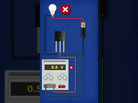
Transistors in Series Problem

Показать описание
Here is of Problem that I ran in to when working on a
AND logic gate
Hope this helps!
for my multimeter video:
for PCBways website:
thanks for watching!
-Daniel
AND logic gate
Hope this helps!
for my multimeter video:
for PCBways website:
thanks for watching!
-Daniel
 0:03:56
Transistors in Series Problem
 0:04:21
Electrical Engineering: Ch 3: Circuit Analysis (34 of 37) Solving Basic Transistor Circuit (MESH) 1
 0:04:57
Transistor circuits
 0:05:40
BJT (Bipolar Junction Transistor) Solved Problem | Quiz # 327
 0:13:57
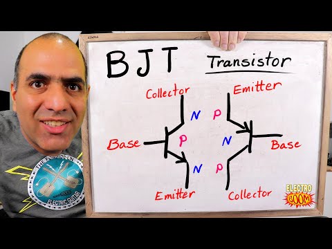
Starter Guide to BJT Transistors (ElectroBOOM101 - 011)
 0:19:14
Electronics tutorial - 3/3 Driving multiple transistors in series
 0:01:00
Transistors Explained - What is a transistor?
 0:03:06
CALCULATING W/L RATIO OF A TRANSISTOR (OR) SIZING OF A TRANSISTOR
 1:11:13
R.T. is LIVE: KoolKlox Nixie/Binary Kit Lets pluck some transistors and test them.
 0:30:17
Transistors - NPN & PNP - Basic Introduction
 0:11:52
Problem on NMOS Pass transistor Logic (GATE 2014 ECE Paper Solution)
 0:01:41
Series connection of transistors in power supplies
 0:08:43
Using a transistor to solve our problem | Digital electronics (8 of 10)
 0:09:15
Circuits 2 - NPN Transistor
 0:27:04
How To Solve Diode Circuit Problems In Series and Parallel Using Ohm's Law and KVL
 0:14:37
Finding Currents and Voltages | Transistor Problems
 0:08:34
Transistor Transistor Logic
 0:01:42
How MOSFET Transistor Works | What It Can do | How to Test It ✔
 0:03:26
Transistor Circuits - Solved Example
 0:04:03
Transistor as a Switch - Bipolar Junction Transistor - Basic Electronics
 0:09:16
Voltage Regulator using Transistor | Series Voltage Regulator | cheap Voltage Regulator
 0:13:31
Find VCE, VBE and VCB of Transistor || BJT Solved Numerical
 0:08:10
Find IB, IC, and vo and in the transistor circuit of Fig Assume that the
 0:10:49
Building logic gates from MOSFET transistors
Комментарии