filmov
tv
How to Use Rooms with Rules in Altium Designer

Показать описание
Rooms allow you to use rules on specific areas of your design. This helps immensely with properly defining trace widths and hole sizes for specific components. Learn how easy it is to assign rules to specific rooms in the PCB with Altium Designer.
0:00 Intro
0:11 What Can a Room be Used for?
1:14 How to Create a Room Rule
2:44 Rule Priority
2:52 Routing with the New Rule
Don't forget to follow us on social to stay up-to-date on the latest Altium Academy content.
The Altium Academy is an online experience created to bring modern education to PCB Designers and Engineers all across the world. Here you can access a vast library of free training and educational content covering everything from basic design to advanced principles and step-by-step walkthroughs. Join industry legends as they share their career knowledge, review real-life design projects, or learn how to leverage one of Altium's leading design tools. No matter your level of experience, the Altium Academy can help you become a better Designer and Engineer!
About Altium LLC
Altium LLC (ASX:ALU), a global software company based in San Diego, California, is accelerating the pace of innovation through electronics. From individual inventors to multinational corporations, more PCB designers and engineers choose Altium software to design and realize electronics-based products.
#Altium #PCBdesign #altiumdesigner
-~-~~-~~~-~~-~-
Check Out Our Latest Video: "How to Draw Antipads"
-~-~~-~~~-~~-~-
 0:03:49
How to Use Rooms with Rules in Altium Designer
 0:04:40
Using Breakout Rooms During a Meeting
 0:05:04
How to use breakout rooms in Microsoft Teams
 0:00:29
Many ways to furnish a 3mx3m room! #smallspace #fengshui #bedroom #dorm #smallapartment #tinyhouse
 0:06:54
HOW TO USE ZOOM BREAKOUT ROOMS IN 6 MINS - FULL DEMO | Complete Tutorial For Beginners
 0:10:37
Rooms in Revit Tutorial
 0:08:30
How to use Teams Breakout Rooms
 0:00:28
types of lighting for the bedroom! which is your favourite? #lighting #bedroom #ambience #nightstand
 0:00:46
⚡️Limited Units !! Ultima 107 Premium Builder Flats in Sector -107, Noida #affordable #home #shorts...
 0:00:41
Tricks to make your bedroom feel calm and balanced and beautiful!
 0:00:30
How to make a long & narrow room feel generous #bigspace #smallspaces #interiordesign #spaceplan...
 0:01:19
How and When to Use Rooms in Altium Designer
 0:06:20
How to find rooms on Housing Portal - WG-Gesucht | Successful flatshare application | WG-Casting
 0:00:16
renovate your room using ai #shorts #ai #aiart #tech
 0:00:16
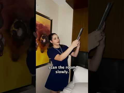
Easy way to look for a hidden camera
 0:04:13
Room Acoustics for Small Rooms - Why do small rooms suffer from bad acoustics?
 0:05:05
How to create rooms and build walls - ROOMTODO - Tutorial
 0:00:18
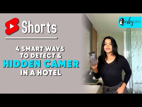
4 Smart Ways To Detect Hidden Cameras In A Hotel | Curly Tales
 0:00:16
Which paint finish should I use? #interiordesign #barrickmandesign
 0:00:25
Paint Hack #shorts
 0:00:30
Small Bedroom Storage Solutions - IKEA Home Tour
 0:02:22
Rooms: The professional remote recording tool in Descript
 0:00:30
Easy DIY wainscoting to add some class to this dining room. #diy #wainscoting #moulding #diyprojects
 0:01:00
How to ALWAYS find Ultra Secret Rooms! #tboi #gaming #bindingofisaacrepentance #isaacrepentance
Комментарии