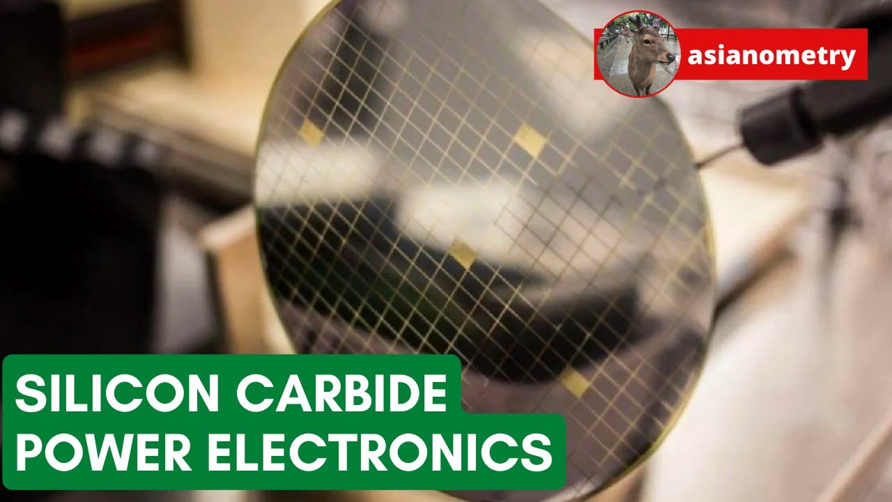
Silicon Carbide: A Power Electronics Revolution

preview_player
Показать описание
In 2018, Tesla inverted our expectations and shook the EV industry when they adopted an ST Microelectronics silicon carbide-based inverter for their new Model 3 Electric Vehicle.

It allowed Tesla to shrink one of an EV's most critical components in half. And it has sparked new interest in a silicon technology as old as the industry itself.

In this video, we are going to take a look at the powerful benefits of silicon carbide-based power semiconductors.

Links:
Рекомендации по теме
Комментарии
Автор

Impressively well researched video for a non electronics specialist. You’ve done a far better job than other commentators on the topics. Love your videos.

rkaid
Автор

Until a few months ago, I was a research fellow working on silicon carbide devices. Please allow me to leave some commentary:

1:40 - 4H and 6H are the only polytypes that can be grown as commercially-relevant bulk wafers, but 3C can be grown on silicon! 3C-on-Si is... well, it's not great. In layman's terms, the atomic spacing of 3C-SiC is different to that of Si, meaning 3C-on-Si is *full* of crystal defects. Just to pile it on, SiC fabrication processes can get up to 1600°C, but Si melts at those temperatures, meaning there's key steps you can't do properly to 3C. I am very interested to see if the 3C wafers devised by Francesco La Via and his team - where they start a 3C layer, melt off the Si and grow a new 3C wafer from the starting layer - can reach the crystal quality and practicality required for real devices. 3C has a bandgap that's not as wide as 4H or 6H, but its electron mobility is higher and it might compete with GaN in lower voltage applications. If La Via and his guys can improve their process!

2:00 - 4H has a wider bandgap than 6H and isn't much harder to grow, that's basically why we're using it.

2:08 - Tangent: the same strong atomic bonding that makes SiC hard also makes it a pain in the butt to chemically etch. Acids don't do anything to it and basically the only way to etch it is high-power plasma etching (plasma etching is common, but SiC needs a serious bombardment before any of it goes away)

2:26 - This explanation is generally pretty good. The wide bandgap of SiC means better temperature tolerance (lower intrinsic carrier concentration) and better voltage blocking, but you glossed over the higher frequency thing (and, TBH, I don't blame you). SiC has a higher electron saturation velocity than Si. Effectively, the electron speed limit is higher. *BUT* while the electron saturation velocity is higher than Si, the electron mobility is *much* lower (and don't even get me started on the hole mobility). The speed limit might be higher, but you've replaced your roads with grass fields. While SiC can *match* Si up to ~10MHz, it's beaten tidily by GaN at radio frequencies.

4:10 - While SiC as a semiconductor tolerates heat much better than Si, there's a reason why SiC transistors aren't rated to higher temperatures and it's *super important*: the oxide of the metal-oxide-semiconductor field effect transistor. I'll cover it in detail below...

6:57 - Partially true. Above 6.5kV, we go into the world of thyristors. Which I don't know that much about, other than 'big, scary whole-wafer devices', so I'll stop.

7:32 - This stuff about heat is a bit misleading. Power semiconductor devices *always* need heat management, but once you've put them in a proper box, the environment is usually less important than what thermal management you put in.

8:09 - You kinda turned over two pages at once here, mate. Batteries do not store as much energy as a tank of fuel and getting a battery electric vehicle to travel as far as an internal combustion engine (ICE) one is very difficult. Also, paradoxically, the high efficiency of electric motors means that small inefficiencies in the car's design turn into bigger losses of range. Those pop-out door handles that sit flush to the car while driving don't really make any difference to an ICE car - which is already pissing away ~80% of its energy - but they do genuinely help with an EV. Thus, adding or saving weight translates more directly into range, which is something EV buyers prize highly while they make the adjustment to EVs and their shorter range.

8:18 - Sorry, this is a pretty big error. Also kinda complicated to unpack, but I'll give it a go. Beyond the transistor itself, building a power converter requires passive components. Capacitors and inductors. Transistors switch almost a million times per second and passive components act as energy reservoirs to smooth out voltage and/or current. The faster the switching speed, the less time the passives need to plug the gap for, and the smaller they can be. When it comes to capacitors and, particularly, inductors, a larger capacitance/inductance value means a physically larger and heavier component. Fast-switching SiC MOSFETs (they switch much faster than a Si IGBT of the same voltage/current rating) mean smaller, lighter, cheaper passive components, and this is where the bulk of the efficiency saving comes from (although faster switching normally also means lower losses in the conversion itself, so higher efficiency and less heat generated).

9:27 - Material growth *is* a major limitation of SiC. It's not the only one, and I need to do a full-length diatribe about oxides below...

10:37 - This breakdown of PVT growth is *excellent*, and I just learned a thing or two about it. This explanation makes the process sound a lot cleaner and less messy than it really is: controlling the temperature gradient around the reactor well enough to create a decent SiC ingot with no polytype inclusions is extremely difficult, and I'm not entirely convinced that another ingot growth method isn't going to replace PVT (/hottake).

11:58 - SiC wafers can be laser cut. I don't know about wafering from an ingot, but it's also possible (if a little risky) to cleave the wafer to dice it, like cutting glass. But just laser cut it.

OK, I need to talk about oxides, not just because they were the topic of my PhD but also because they're the weakest part of a SiC MOSFET. When making a metal-oxide-semiconductor stack for a silicon transistor, you use the silicon as a ingredient for the oxide. Stick a clean wafer in a hot furnace with oxygen flow and it will slowly oxidise to a very clean, orderly silicon dioxide. When you try to do this with SiC, for a few nanometres you get Si oxidising to SiO2 and C burning off as CO2, but the carbon quickly ends up trapped in the oxide and at the oxide-semiconductor interface. This tanks the performance of the oxide. There are moderately-effective ways of un-tanking the performance - using NO or N2O as the oxidising gas, instead of oxygen - but they're still much worse than for Si devices. The on-state resistance of SiC MOSFETs is limited by the quality of the gate oxide and the MOSFET channel it produces. The maximum temperature is limited by the reliability of the oxide: up to 175°C, the oxide is OK, but above that its lifetime shortens drastically. My pet project during my postdoc (which I've still got a successor working on, which I am super-grateful for) was depositing SiO2 rather than oxidising the Si. You can't trap any carbon if you leave it all in the semiconductor. Instead, you have different problems, like oxygen vacancies in the oxide. I should stop.

Thanks for sharing. This video is a good introduction and overview of device technologies that you don't see in popular engineering. Good stuff!

gigabyte
Автор

John Atanasoff, inventor of the Atanasoff-Berry computer, one of the very early stored program digital electronic computers, talked in a speech at the Computer History Museum about theorizing about building transistors out of silicon carbide as far back as the 1930s. He knew that both galena (lead sulfide) and silicon carbide could serve as a cat's whisker crystal detector in a radio set. When they were improperly adjusted, they would oscillate, and oscillation means gain/amplification. Interesting that silicon carbide semiconductors are now a commercial product. Atanasoff envisioned making them out of what we would call nanowires.

gregorymalchuk
Автор

About carbide hardness: tungsten carbide is used in good ballpoint and gel roller pens as the ball. It sees a lot of wear and needs to remain smooth and spherical to apply ink evenly

cFyugThCzvAqYaGmxRgfCKTuvHMEjQ
Автор

Another great video. Being an engineer this was very easy to understand, but I think your explanation still bought a lot of easy to understand points to the Lay person. Your walk through the history of the materials and technology is also most important for the younger viewer (I do hope you have many young viewers). Thanks.

KarelSeeuwen
Автор

As a college undergrad in 1991 I worked in a university (University of Florida) research lab doing preparation and characterization of Silicon Carbide deposited layers onto various materials. Our method was chemical vapor deposition whereby a graphite holder inside of a quartz tube surround by outside copper coils with cooling water running through them would be subjected to an A/C current. As the magnetic fields changed polarity many times per second the graphite crystal layers would react to the changing magnetic fields and thereby induce heating through the friction associated with the graphite layers "rubbing" against each other. It was so long ago now I don't remember the exact temperature but I do remember the graphite would begin to glow after a short while. The substrate (Alumina if I recall) we planned to deposit the SiC on was placed on the graphite holder during assembly and consequently would also get heated to exceedingly high temps. Once the entire assembly was up to temp I would inject into the reactor a steady flow of Hydrogen (H2) gas bubbled through a silicon tetrachloride solution. The SiCl4 would diffuse into the hydrogen and be transported into the reaction chamber and them a constant stream of methane (CH4) gas was used as the source for carbon in the experiment. The high heat energies would rip apart the molecules and you would then have a gaseous phase of carbon, silicon, chlorine and other elements above the substrate. Some fraction of these materials would react to form Silicon-Carbide (SiC) that gets deposited onto the substrate. The whole purpose of the experiments were to characterize the regime under which you maximized SiC production and minimized other undesired reactions. For that we would have to take the samples to the materials science department on campus where we could use their SEM to check the deposited layers for purity. All of this work went on for years and formed the basis of a PhD thesis for a graduate student I was working with. It was also funded by DARPA principally as a means to identify coatings that could be used in tank engine components to protect them from wear and corrosion. Never did I imagine there would be a use for this material as a semiconductor. Although I have to say it makes sense because the professor who was the PI for all these research projects was a specialist in semiconductor materials.

caseroj
Автор

Consistently impressed with how you distill technical topics into their essence, explaining enough detail that a scientist can understand while a layperson can follow along. Another disruptive application of SiC is in electric kilns, nichrome wire barely gets to 1200C, SiC filaments can get up to 1600C. Would be critical for decarbonizing heavy industry like cement and aluminum. One of the issues in this field is also with scale of heater elements.

Dr_Petey_Wheatstraw
Автор

I don’t find many videos out there that dive into details of semiconductors like this. As chip designer I actually learned things from your video. Please, continue the great work you have been doing in this channel.

alirezaseyfollahi
Автор

Hey Asianometry, just wanted to give a quick thank you for your videos. As a new salesperson to the semiconductor industry, these videos are extremely helpful on providing info about the semiconductor industry as a whole, as well as explaining the different technologies/processes involved. Thanks again and keep it up!

natenotnathan
Автор

Thank you for giving me an introduction in this technology as I work for Inverters in the automotive industry. This really was a useful introduction to something everybody speaks of, but nobody dares to really explain

motivase
Автор

This is why I Love this channel, I always learn something new about industry with a little dash of humor on the side.

hexwrench
Автор

@7:41 I don't think many people in the world would recognize that! It's the underside of an older Proterra bus. Having worked on them in wintry cities, I can confirm that those are some harsh conditions indeed.

ElectricNed
Автор

5:13 I love that this particular Tesla is from a slovak town Senec with population of ca. 20 000 people.

micgalovic
Автор

I took one condensed matter/solid state physics course in college and this video was very digestible, I would say even for people without the physics background.

mrnarason
Автор

Wonderful!
Can you also explain the Galium Nitride (GAN) transistors and how they compare to Silicon Carbide and other power switching devices.
GANs are apparently also finding their way into power electronics lately.

PeterKese
Автор

A new step in semiconductor tech. Brilliant video, thank you.

tommiller
Автор

You often mention "packaging" which means something different than what most people normally would understand it to be (cardboard boxes and styrofoam). Can you do a video on the meaning of "packaging" throughout the semiconductor industry?

Keavon
Автор

Multiple people have mentioned doing a video on GaN, I'd love that too.
Another worthwhile topic relates to that graph about growth in the power electronics device use - the insane backlog in getting devices. There a cracks in the supply / demand when it comes to processors and other devices, but the high backlogs on power electronics looks solid.

matthewbeasley
Автор

Finally SiC!!!! .. Im Ph.D student and I'm working with silicon carbide.. Finally a video about that!

renatoberaldo
Автор

Following you already a long time and was wondering when you do the video about one of the most powerful changes in the industry for high power applications. I am working for an SiC Semiconductor manufacturer and i think you did a great job explaining the technology. Short correction traditional silicon mosfets work up to 100V max.

dadude
welcome to shbcf.ru