filmov
tv
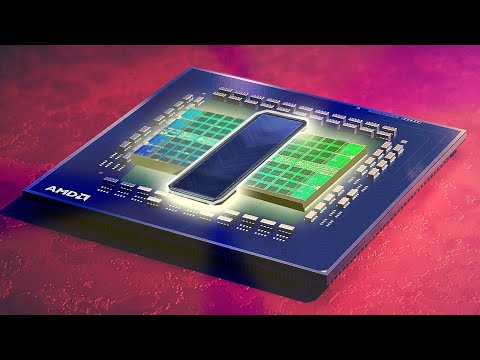
AMD 7900XT's CHIPLETS are a bit different

Показать описание
I now stream at:
Footage from various sources including official youtube channels from AMD, Intel, NVidia, Samsung, etc, as well as other creators are used for educational purposes, in a transformative manner. If you'd like to be credited please contact me
#AMD #CHIPLETS #NAVI31
 0:07:32
AMD 7900XT's CHIPLETS are a bit different
 0:05:46
AMD’s RX 7900 XT Will Have 7 CHIPLETS (Dies)?
 0:06:29
AMD in de aanval - RX 7900 XT(X) Review
 0:07:46
AMD Just Changed the Game - GIANT RX 7900 XT GPU Leak
 0:11:40
Best gaming value on the market? AMD Radeon RX 7900 XTX and 7900 XT Review
 0:17:06
Next Gen GPUs? CHIPLETS!
 0:26:46
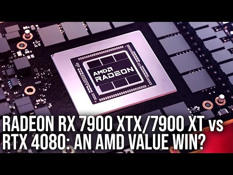
Radeon RX 7900 XTX/ RX 7900 XT vs RTX 4080 Review: Can AMD Bring The Value?
 0:09:33
Can AMD Radeon RX 7900 XT beat RTX 4090?
 0:23:54
AMD’s 7900 XT and 7900 XTX TESTED! Is RDNA 3 The New Price/Performance KING?
 0:10:14
Navi 31 has SEVEN chiplets?! Here’s how
 0:10:36
AMD is FINALLY useful for streamers & creators?!
 0:05:35
Should You Buy A Radeon RX 7900?
 0:20:40
This video will not age well... - AMD Radeon RX 7900 Series Review
 0:09:58
RX 7900XT: WARNING: Big numbers! (and questions about ray tracing)
 0:06:47
The RX 7900XT's 3D Chip Will be AWESOME!
 0:01:42
Introducing AMD Radeon™ RX 7900 XTX
 0:09:04
AMD FINALLY WINS - GIANT RX 7900 XT Leak
 0:16:26
How AMD is Fighting NVIDIA with RDNA3 - Chiplet Engineering Explained
 0:27:38
AMD RX 7900 XTX Analysis: RDNA 3 & RDNA 4 Economics are TROUBLE for Nvidia (+ RTX 4080 Supply Le...
 0:18:32
What I Like and DON'T Like about the 7900 XTX Launch.
 0:04:15
AMD Radeon RX 7900 XTX and 7900 XT RDNA3 Graphics Cards Launched
 0:00:26
AMD Radeon RX 7900XTX | RX 7900 XT | Price | Specs | 8k Gaming | Release Date | RDNA 3 Highlights
 0:26:22
Radeon RX 7900 XTX, 7900 XT And RDNA 3 LIVE Chat With AMD!
 0:06:36
AMD’s Chiplet RDNA 3 GPU’s are Getting Closer!
Комментарии