filmov
tv
(9) Generating Fabrication Files - Altium Designer

Показать описание
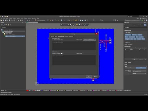
In this final episode of the Altium Designer Getting Started Tutorial, we finish up with the all-important process of generating manufacturing outputs for getting your new PCB design made. This video will show you how to generate gerber, N.C. Drill and other fabrication file formats, and assembly documents such as Pick-and-Place files and Bills of Materials. Upon completion of this tutorial module, you have walked through the entire design process from scratch, starting with nothing and ending with a completed design with manufacturing output files.
(9) Generating Fabrication Files - Altium Designer
9. Generating Fabrication Files
Generating Fabrication Files | Altium Designer 17 Essentials | Module 26
altium gerber file generation | Tutorial for Altium Beginners: Generating Manufacturing Outputs
How To Generate Fabrication Files In Altium Designer | Gerber | Pick & Place | Detailed Explanat...
3 Types Of PCB Manufacturing Output Files You Need To Know
Tutorial 5 for Altium Beginners: Generating Manufacturing Outputs
Altium Designer v22 How to Automatically Create Manufacturing Files
How To Generate Fabrication Files In Altium Designer | Gerber File For PCB Assembly
How To Generate Fabrication Files In Altium Designer | Gerber | Pick & Place | Detailed Explanat...
How to Generate Manufacturing Files in OrCAD PCB Editor 17.4
Altium Tutorial Beginner VID13 -How to generate manufacturing files old and new style (Output job)
Communicating Design Intent with Manufacturing Outputs
Gerber data for PCB fabrication | Allegro PCB Designer
1-Click to Output Manufacturing Files
21 KiCad Tutorial: Converting PCB Files to Gerber Format for Manufacturing
Autodesk Revit MEP 2016: Export Duct and Nest for Fabrication
Miter Elbow Calculation/ Fabrication Formula
Generating Manufacturing Data for your PCB Designs
CRISPR Explained
Live Webinar: Output Job Files for Rapid, Repeatable PCB Manufacturing Data Generation
Microcontroller-Based Hardware Design With Altium Designer - #10 Manufacturing Files
Limitless Manufacturing Group presents - Submitting designs, mock-ups, and tech packs to manufacture
Team Phantom - Altium Tutorial #12: Generating PCB manufacturing outputs
Комментарии
 0:03:45
 0:03:24
 0:12:21
 0:09:58
 0:20:18
 0:12:45
 0:59:34
 0:09:50
 0:17:57
 0:26:21
 0:01:21
 0:27:36
 0:18:49
 0:03:19
 0:03:55
 0:04:34
 0:01:02
 0:04:31
 0:35:43
 0:01:39
 0:27:48
 0:11:58
 0:01:01
 0:09:47