filmov
tv
How to make PCB using MARKER PEN (Printed Circuit Board)
Показать описание
How to make PCB using MARKER PEN (Printed Circuit Board)
Please Like & Share. Thanks for subscribing.
Visit DIY Projects Channel for more Cool Videos
© 2018 DIY Projects All Rights Reserved
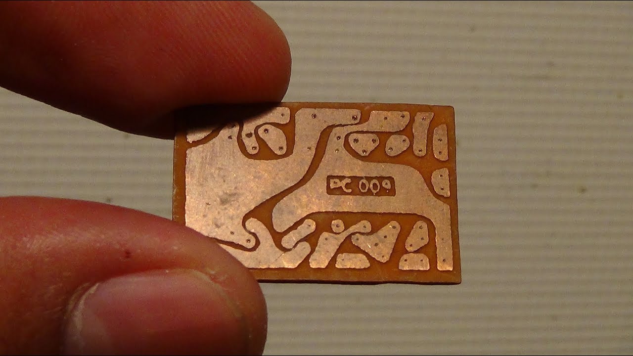
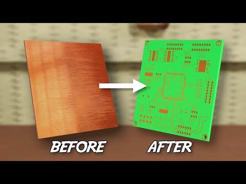
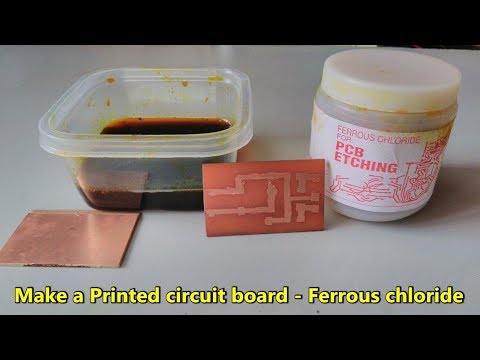
A printed circuit board, or PCB, is used to mechanically support and electrically connect electronic components using conductive pathways, tracks or signal traces etched from copper sheets laminated onto a non-conductive substrate. When the board has only copper tracks and features, and no circuit elements such as capacitors, resistors or active devices have been manufactured into the actual substrate of the board, it is more correctly referred to as printed wiring board (PWB) or etched wiring board. Use of the term PWB or printed wiring board although more accurate and distinct from what would be known as a true printed circuit board has generally fallen by the wayside for many people as the distinction between circuit and wiring has become blurred. Today printed wiring (circuit) boards are used in virtually all but the simplest commercially produced electronic devices and allow fully automated assembly processes that were not possible or practical in earlier era tag type circuit assembly processes.
Just in 5 simple steps
A PCB populated with electronic components is called a printed circuit assembly (PCA), printed circuit board assembly, or PCB Assembly (PCBA). In informal use, the term "PCB" is used both for bare and assembled boards, the context clarifying the meaning. The IPC preferred term for populated boards is CCA, circuit card assembly.[1] This does not apply to backplanes; assembled backplanes are called backplane assemblies by the IPC.
Alternatives to PCBs include wire wrap and point-to-point construction. PCBs must initially be designed and laid out, but become cheaper, faster to make, and potentially more reliable for high-volume production since production and soldering of PCBs can be automated. Much of the electronics industry's PCB design, assembly, and quality control needs are set by standards published by the IPC organization.
how to make PCB using a marker pen
how to make pcb at home
© 2013 HadronMesons All Rights Reserved
Benyamin Amiri
Please Like & Share. Thanks for subscribing.
Visit DIY Projects Channel for more Cool Videos
© 2018 DIY Projects All Rights Reserved
A printed circuit board, or PCB, is used to mechanically support and electrically connect electronic components using conductive pathways, tracks or signal traces etched from copper sheets laminated onto a non-conductive substrate. When the board has only copper tracks and features, and no circuit elements such as capacitors, resistors or active devices have been manufactured into the actual substrate of the board, it is more correctly referred to as printed wiring board (PWB) or etched wiring board. Use of the term PWB or printed wiring board although more accurate and distinct from what would be known as a true printed circuit board has generally fallen by the wayside for many people as the distinction between circuit and wiring has become blurred. Today printed wiring (circuit) boards are used in virtually all but the simplest commercially produced electronic devices and allow fully automated assembly processes that were not possible or practical in earlier era tag type circuit assembly processes.
Just in 5 simple steps
A PCB populated with electronic components is called a printed circuit assembly (PCA), printed circuit board assembly, or PCB Assembly (PCBA). In informal use, the term "PCB" is used both for bare and assembled boards, the context clarifying the meaning. The IPC preferred term for populated boards is CCA, circuit card assembly.[1] This does not apply to backplanes; assembled backplanes are called backplane assemblies by the IPC.
Alternatives to PCBs include wire wrap and point-to-point construction. PCBs must initially be designed and laid out, but become cheaper, faster to make, and potentially more reliable for high-volume production since production and soldering of PCBs can be automated. Much of the electronics industry's PCB design, assembly, and quality control needs are set by standards published by the IPC organization.
how to make PCB using a marker pen
how to make pcb at home
© 2013 HadronMesons All Rights Reserved
Benyamin Amiri
 0:10:40
PCB Creation for Beginners - Start to finish tutorial in 10 minutes
 0:05:35
DIY PCB Fabrication (Dry Film Inkjet Method)
 0:04:09
How to Design & PCB Etching- Part 2
 0:00:16
Etching PCB At Home #shorts
 0:00:16
PCB Design #pcbdesign #electronics
 0:06:08
What is a PCB?
 0:05:42
How To Make a Printed Circuit Board (PCB) using Ferric Chloride and Maker pen
 0:00:11
Free PCB Design Software
 0:19:46
RP2350 Hardware PCB Design in KiCAD | Custom RP2350 Schematic & PCB Design
 0:19:56
How It's Made: Multilayer PCB Manufacturing Insight
 0:09:28
How To Make Custom PCB's For Your Projects!
 0:12:23
You can now PRINT PCBs! Creating a homemade PCB with the Voltera V-One PCB Printer!
 0:00:16
PCB Design in Easyeda #pcbdesign||Easyeda tutorial #electronics#ece#pcb
 0:05:32
how to make pcb at home with Laser xTool F1, DIY PCB Fabrication
 0:03:33
Just print a PCB (HOW TO)
 0:10:27
What are PCBs? || How do PCBs Work?
 0:00:08
Received PCB From Various Manufacturers - KiCad 7 tutorial series #pcb #electronics
 0:13:16
KiCAD 7 PCB Layout in 5 steps
 0:08:16
How to easily design PCB in EasyEDA software
 0:00:08
Remember To Use Flux When Soldering Header Pin onto a Prototype Board!
 0:10:44
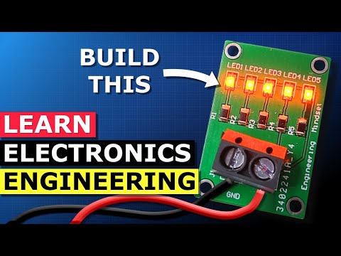
Design and Build a PCB - SMD LED Learn electronics engineering
 0:00:16
3D Printed Business Card Embosser Roller PCB Style
 0:00:59
Best and Worst PCB Design Software
 0:00:27
Make your own PCB's on your 3D Printer
Комментарии