filmov
tv
300 mm Semiconductor Cleanroom Tour 2024 | Fraunhofer IPMS

Показать описание
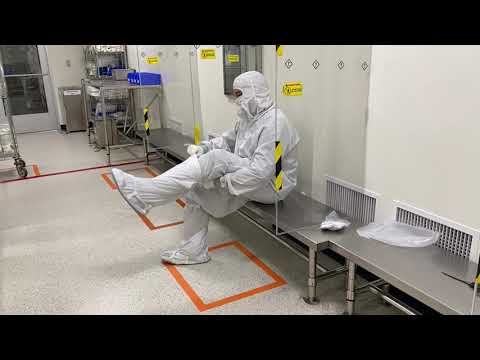
Follow us for a look into the 300 mm cleanroom of Fraunhofer IPMS. Dr. Benjamin Lilienthal-Uhlig, Head of Business Unit Next Generation Computing, will show you state-of-the-art equipment for semiconductor technology in a short guided tour.
300 mm Semiconductor Cleanroom Tour | Fraunhofer IPMS
300 mm Semiconductor Cleanroom Tour 2024 | Fraunhofer IPMS
Intel Fab 28 Tour- Clean Room Material Handling System Picking Up a FOUP
The 300mm Silicon Wafer Transition
Intel Fab 28 Tour Clean Room Material Handling System
Intel Fab 28 Tour- Clean Room Material Handling System in Action
Cleanroom where IISc-startup International Center for Nanodevices manufactures nanoDs
Unveiling High NA EUV | ASML
Intel's Fab 42: A Peek Inside One of the World’s Most Advanced Factories
Semiconductor Clean Room Design Requirements 101 | Air Innovations
A Day in the Life of a Clean Room Technician
#300mm Silicon #Wafer Manufacturing Process
‘Semiconductor Manufacturing Process’ Explained | 'All About Semiconductor' by Samsung Sem...
How are BILLIONS of MICROCHIPS made from SAND? | How are SILICON WAFERS made?
Semiconductor Cleanroom Tools: Introducing Lesker PVD200 load deposition system | Fraunhofer IPMS
I Can Die Now. - Intel Fab Tour!
Nicole Scott visits the new Bosch 300mm semiconductor fab in Dresden, Germany
Automated Material Handling Systems Solution (Semiconductor)
SEMICONDUCTOR WAFER WET CLEANING
How are Microchips Made? 🖥️🛠️ CPU Manufacturing Process Steps
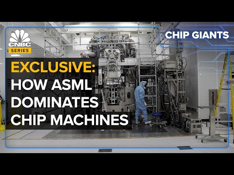
Why The World Relies On ASML For Machines That Print Chips
RF GaN Experience | Fab Tour
Take A Sneak Peek Inside an Intel Sub Fab
Meet Rachel Harrington, Cleanroom Technician | ASML US
Комментарии
 0:05:10
 0:05:21
 0:00:10
 0:15:00
 0:00:09
 0:01:18
 0:00:12
 0:01:39
 0:02:45
 0:01:47
 0:03:01
 0:04:20
 0:07:44
 0:08:40
 0:00:44
 0:21:51
 0:05:27
 0:03:01
 0:00:57
 0:27:48
 0:18:40
 0:03:09
 0:03:02
 0:01:19