filmov
tv
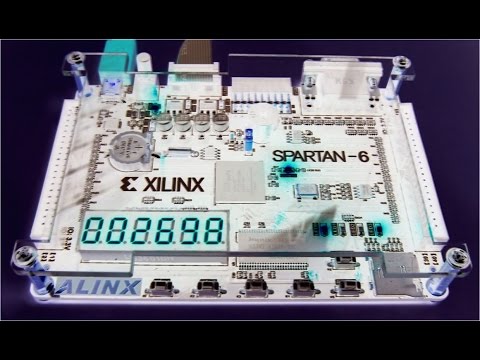
FPGA Development Tutorials | Alinx AX7020 | Zynq7000 Architecture

Показать описание
Want to know about What is FPGA and FPGA Development Process. Details of Zynq7000 Architecture and its functional Block Diagram. How to write your very first Verilog code for FPGA Development using Xilinx Vivado Design Suite. For all this we are going to use ALINX AX7020 Development kit.
🎥Video Timeline:
[00:00] Video Introduction
[01:05] What is FPGA?
[01:40] Explanation of Zynq 7000 Architecture
[05:59] 16 Steps Process of FPGA Development
[08:29] Setting Vivado Development Environment in Windows
[10:57] SD-Card and JTAG Configuration Jumper
[11:40] Create First FPGA Development Project
[14:48] Write LED Blinking Verilog code using 50Mhz Ref Clock and Counter
[24:26] Define the I/O Pins and Create Constraints File ".XDC"
[27:39] Define Timing Constraints for 50Mhz sys_clk
[29:14] Run Synthesis and Generate Bit Stream file
[30:17] Open Hardware manager and Program the AX7020 FPGA Development kit
▬▬▬▬▬▬▬▬▬▬▬▬▬▬▬▬▬▬▬▬
✦ Important Links:
▬▬▬▬▬▬▬▬▬▬▬▬▬▬▬▬▬▬▬▬
ALINX AX7020 Development Kit for this tutorial series:
Vivado Design Suite - HLx Editions - 2020.2 Full Product Installation:
Zynq 7000 devices Documentations:
▬▬▬▬▬▬▬▬▬▬▬▬▬▬▬▬▬▬▬▬
✦ EsteemPCB Courses on Udemy:
▬▬▬▬▬▬▬▬▬▬▬▬▬▬▬▬▬▬▬▬
 0:32:18
FPGA Development Tutorials | Alinx AX7020 | Zynq7000 Architecture
 0:08:12
fpga development tutorials alinx ax7020 zynq7000 architecture
 0:22:36
FPGA Development Tutorial | Alinx AX7020 | Phase Locked Loop PLL in FPGA
 0:13:01
FPGA Development Tutorial | Alinx AX7020 | Switch and Push Button Debouncing using D Flip-Flops
 0:01:45
AX7A200: The Ultimate FPGA Development Board for PCIe Solutions, Video Processing, and More!
 0:19:38
FPGA Simulation and Debugging Tutorial | Alinx AX7020 | ILA IP Core Application
 0:00:32
Alinx products
 0:00:34
A Cheap ALINX XILINX FPGA Board
 0:00:54
RF Modulation Recognition on AMD-Xilinx ZYNQ UltraScale+ FPGA device
 0:02:01
UberDDR3 + OpenXC7: Alinx AX7103B FPGA Demo Project
 0:01:57
AX7020: The Ultimate Zynq-7000 SoC FPGA Development Board
 0:00:36
Alinx Xilinx Kintex-7 FPGA Development board
 0:03:10
XILINX A7 FPGA Development Board Artix-7 XC7A35T: The Ultimate FPGA Platform for Enthusiasts
 0:01:13
HDMI OUT Photo slideshow using EDGE ZYNQ SoC FPGA kit
 0:07:20
Intel® Agilex™ FPGA CXL IP
![[AX7035 FPGA bOARD]29](https://i.ytimg.com/vi/fKfv7cjG-8g/hqdefault.jpg) 0:15:17
0:15:17
[AX7035 FPGA bOARD]29 USB Two way Speed Measurement Experiment
 0:00:28
FPGA: Mojo v3 - Sound detection servo platform
 0:00:36
Down counter implemented on FPGA board
 0:09:54
Kintex-7 XC7K325T FPGA Development Board Overview
 0:04:17
Demonstration of Teledyne e2v DDR4 with AMD XILINX Kintex Ultrascale FPGA
 0:00:16
MiSTeryNano #9: Tang Nano 20k as USB host #retrogaming
 0:03:13
XC7Z015 1CLG485C#Xilinx Datasheet
 0:11:47
BIST Test Kintex-7 FPGA XC7K325T-2FFG900C FPGA (KC705)
 0:00:17
FPGA firmware developed by LabVIEW in a non-NI FPGA board
Комментарии