filmov
tv
Lab #20 DC Analysis VTC of NMOS | AKTU | Orcad 16.6 lite simulation software | electronics branch

Показать описание
Exp 3c: DC Analysis (VTC) of NMOS Inverter with and without parameters.
Exp 1: Introduction of OrCAD and PSpice.
Exp 2a: Transient Analysis of BJT Inverter using step input.
Exp2b: DC Analysis (VTC) of BJT Inverter with and without parameters.
Exp 3a: Transient Analysis of NMOS Inverter using Step Input.
Exp 3b: Transient Analysis of NMOS Inverter using Pulse Input.
Exp 4a: Transient Analysis of CMOS Inverter using Step Input.
Exp 4b: Transient Analysis of CMOS Inverter using Step Input with Parameters.
Exp 4c: Transient Analysis of CMOS Inverter using Pulse Input.
Exp 4d: Transient Analysis of CMOS Inverter using Pulse Input with parameters.
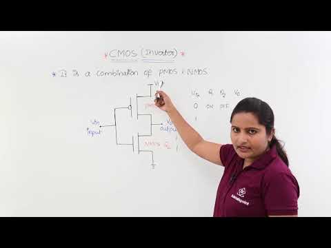
Exp 4e: DC Analysis (VTC) of CMOS Inverter with out parameters.
Exp 4f: DC Analysis (VTC) of CMOS Inverter with parameters.
Exp 5a: Transient Analysis of NOR Gate Inverter.
Exp 5b: DC Analysis of NOR gate Inverter.
Exp 6a: Transient Analysis of NAND Gate.
Exp 6b: DC Analysis of NAND gate.
Exp 7: Design and Simulation of a Differential Amplifier with resistive load and current source biasing.
Exp8: Analysis of Frequency response of common source amplifier.
Exp9: Analysis of Frequency response of source follower amplifier.
Exp10: Analysis of Frequency response of cascade amplifier.
Exp11: Analysis of Frequency response of Differential amplifier.
#diplomatech #cadence #DC_Analysis_(VTC)_of_NMOS _nverter_with_and_without_parameters
Exp 1: Introduction of OrCAD and PSpice.
Exp 2a: Transient Analysis of BJT Inverter using step input.
Exp2b: DC Analysis (VTC) of BJT Inverter with and without parameters.
Exp 3a: Transient Analysis of NMOS Inverter using Step Input.
Exp 3b: Transient Analysis of NMOS Inverter using Pulse Input.
Exp 4a: Transient Analysis of CMOS Inverter using Step Input.
Exp 4b: Transient Analysis of CMOS Inverter using Step Input with Parameters.
Exp 4c: Transient Analysis of CMOS Inverter using Pulse Input.
Exp 4d: Transient Analysis of CMOS Inverter using Pulse Input with parameters.
Exp 4e: DC Analysis (VTC) of CMOS Inverter with out parameters.
Exp 4f: DC Analysis (VTC) of CMOS Inverter with parameters.
Exp 5a: Transient Analysis of NOR Gate Inverter.
Exp 5b: DC Analysis of NOR gate Inverter.
Exp 6a: Transient Analysis of NAND Gate.
Exp 6b: DC Analysis of NAND gate.
Exp 7: Design and Simulation of a Differential Amplifier with resistive load and current source biasing.
Exp8: Analysis of Frequency response of common source amplifier.
Exp9: Analysis of Frequency response of source follower amplifier.
Exp10: Analysis of Frequency response of cascade amplifier.
Exp11: Analysis of Frequency response of Differential amplifier.
#diplomatech #cadence #DC_Analysis_(VTC)_of_NMOS _nverter_with_and_without_parameters
 0:07:03
 0:08:12
 0:05:43
 0:08:09
 0:06:11
 0:04:57
 0:08:36
 0:06:25
 0:07:02
 0:09:00
 0:10:09
 0:28:22
 0:06:21
 0:04:55
 0:10:49
 0:02:30
 0:13:01
 0:02:14
 0:08:17
 0:08:58
 0:25:10
 0:01:14
 0:26:31
 0:00:11