filmov
tv
Samsung Electronics Breaks Ground on New Semiconductor R&D Complex in Giheung, Korea
Показать описание
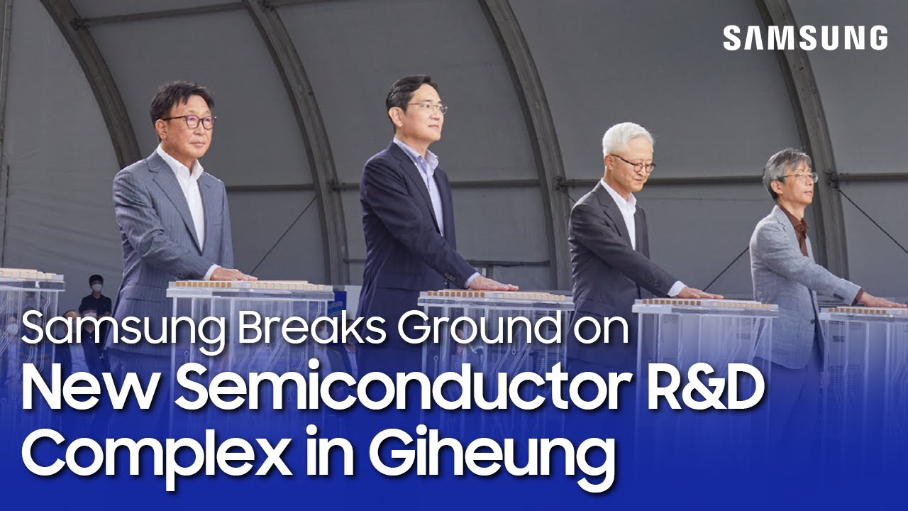
Samsung Electronics today broke ground for a new semiconductor research and development complex in Giheung, Korea, aiming to extend its leadership in state-of-the-art semiconductor technology.
Samsung Electronics plans to invest about KRW 20 trillion by 2028 for the complex in an area covering about 109,000 square meters within its Giheung campus. The new facility will lead advanced research on next-generation devices and processes for memory and system semiconductors, as well as development of innovative new technologies based on a long-term roadmap.
Today's groundbreaking ceremony was attended by Samsung Electronics Vice Chairman Jay Y. Lee, President and CEO Kye Hyun Kyung, President of the Memory Business Jung-Bae Lee, President of the Foundry Business Siyoung Choi, and President of the S.LSI Business Yong-In Park, along with more than 100 employees.
The new Giheung R&D facility, together with the R&D line in Hwaseong and the world’s largest semiconductor production complex in Pyeongtaek, is also expected to elevate the synergy among Samsung’s three main semiconductor complexes in the metropolitan area.
✓ 00:00 Samsung Electronics broke ground for a new semiconductor research and development complex in Giheung, Korea, aiming to extend its leadership
✓ 00:49 Groundbreaking ceremony was attended by Samsung Electronics Vice Chairman Jay Y. Lee
✓ 02:02 The new Giheung R&D facility is also expected to elevate the synergy among Samsung’s three main semiconductor complexes in the metropolitan area.
#Samsungsemiconductor #Technology #Semiconductor
 0:02:55
Samsung Electronics Breaks Ground on New Semiconductor R&D Complex in Giheung, Korea
 0:02:22
Wanna Break New Ground? (with Samsung Display)
 0:01:34
Samsung breaks ground on 3rd biopharmaceutical factory in S. Korea
 0:00:31
Samsung Electronics launches world's fastest graphics DRAM
 0:02:53
Samsung breaks ground on the 7nm foundry that will cast the Galaxy S10 and Note 10 chipsets
 0:00:12
Samsung galaxy S24 FE - a ground breaking smartphone
 0:01:58
Samsung breaks ground on 3rd biopharmaceutical factory in S. Korea
 0:00:36
Samsung Electronics introduces ground-breaking QLED 8K TV at IFA 2018
 0:02:11
Samsung Galaxy S24 FE Debuts In India
 0:00:10
SAMSUNG HIT THE GROUND #SHORTS #SAMSUNG
 0:02:07
Samsung Electronics unveils new environmental strategy, aims to be carbon neutral by 2050
 0:07:09
Samsung's New Worldwide Headquarters Ground Breaking Ceremony
 0:05:36
Workers at Samsung Electronics Walk out for the First Time Ever | Vantage with Palki Sharma
 0:02:11
Samsung Electronics introduces ground-breaking QLED 8K TV at IFA 2018
 0:06:05
Dropping Samsung Galaxy Fold vs iPhone 11 Pro Max vs Nokia 3310 Down Spiral Staircase - 20 Stories
 0:00:40
Samsung Electronics sets out to build 11 semiconductor plants in Texas over next 20 years
 0:00:18
Samsung Galaxy S22 Ultra Drop Test #shorts
 0:00:36
😨samsung s24 ultra vs samsung s23 ultra speed test😱
 0:02:43
Samsung Electronics' Labor Union Says Prepared to Strike ‘Indefinitely’
 0:01:57
Breaking Ground with Samsung Galaxy S24 Ultra: Unboxing and First Look!
 0:01:16
Breaking Ground: The Next Era with Samsung Galaxy S24 Ultra Unboxed!
 0:00:11
Samsung Unveils Odyssey Neo G9 monitor
 0:04:57
Samsung | Fair Electronics Ground Breaking ceremony AV
 0:17:40
The Untold Story Of Samsung’s Growing Chip Business
Комментарии