filmov
tv
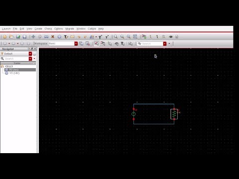
Cadence IC615 Virtuoso Tutorial 16: Layout of Padframe (Part 1/2)

Показать описание
In this tutorial, I have explained the procedure to design the layout of the pads and padframe in Cadence.
 0:17:07
Cadence IC615 Virtuoso Tutorial 16: Layout of Padframe (Part 1/2)
 0:13:04
Cadence IC615 Virtuoso Tutorial 15: Monte Carlo Analysis in Cadence
 0:11:54
Cadence IC615 Virtuoso Tutorial 2 (HD): Symbol Creation and Display Operating points
 0:07:04
Cadence IC615 Virtuoso Tutorial 13: Gain Compression, Harmonic Distortion and THD analysis
 0:10:45
Cadence IC615 Virtuoso Tutorial 17: Using Padframe in circuit design (Part 2/2)
 0:18:51
Cadence IC615 Virtuoso Tutorial 1 (HD): Schematic Entry and Using ADEL
 0:18:46
Cadence IC615 Virtuoso Tutorial 3 (HD): Using Calculator in ADEL
 0:13:07
Cadence IC615 Virtuoso Tutorial 10:Process Corner Simulation in Cadence ADEXL
 0:14:25
Cadence IC615 Virtuoso Tutorial 12: S-parameter analysis in Cadence ADEL
 0:08:32
Cadence IC615 Virtuoso Tutorial 9: Noise Analysis in Cadence ADEL
 0:12:46
Analog Design in Cadence using Virtuoso Tool
 0:12:03
Cadence IC6.16/6.17 Virtuoso Tutorial -1 part 3 (Power calculation use of stimuli)
 0:33:43
Cadence IC6.16/6.17 Virtuoso Tutorial -1 Part 2 (Simulation, Analysis and calculator use)
 0:10:05
Cadence Virtuoso: Introduction
 0:01:34
AND Output waveforms using CADENCE virtuoso
 0:22:24
Introduction to the New Virtuoso ADE Product Suite -- Cadence Design Systems
 0:03:14
Virtuoso ADE Explorer, Assembler & Verifier by Cadence Education Services & Custom IC/Analog...
 0:03:02
Cadence-16: DRC of Layout in Calibre | Design Rule Check (DRC) || Post Layout Simulation
 0:06:53
ECE468 Cadence Virtuoso tutorial -
 0:02:11
OR output for schematic test using CADENCE virtuoso
 0:13:18
Importing PTM 7nm , 16 nm , 22 nm CMOS Technology files Into Virtuoso Cadence®.
 0:10:31
Cadence IC615 Virtuoso Tutorial 5 (HD): Post Layout Simulation, Comp & Finding no of Parasitics
 0:03:21
Sneak Peek - Cadence Virtuoso Workshop
 0:07:05
Cadence 6 Tutorial 13e Extraction
Комментарии