filmov
tv
JFET Biasing: Fixed Bias Configuration Explained (with Solved Examples)

Показать описание
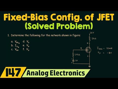
In this video, the Fixed- Bias Configuration of JFET is explained with solved examples.
By watching this video, you will learn the following topics:
0:31 What is Biasing and Different Regions of Operation of JFET
4:40 JFET Fixed Bias Configuration (Circuit Analysis)
8:51 Example 1
13:35 Example 2
17:33 Example 3 (p-channel JFET Example)
What is Biasing?
Biasing is the process of establishing the proper operating voltage and current in the circuit, such that the JFET can be operated in the specific region (Active, linear or cut-off) for a particular application.
In this video, the fixed bias configuration of the JFET and its circuit analysis has been explained. And three different examples have been solved for the fixed bias configuration.
The other videos related to Field Effect Transistor (FET):
1. What is Field Effect Transistor (FET)?
2. Construction and Working JFET
3. Transfer Characteristics of JFET
This video will be helpful to all the students of science and engineering in understanding the Fixed Bias Configuration of the JFET.
#JFETBiasing
#FixedBiasConfiguration
#JFETSolvedExamples
Follow me on YouTube:
Follow me on Facebook:
Follow me on Instagram:
Music Credit:
 0:07:53
Fixed-Bias Configuration of JFET (Mathematical Approach)
 0:23:11
JFET Biasing: Fixed Bias Configuration Explained (with Solved Examples)
 0:02:39
JFET Biasing: Fixed Bias Circuit | Fixed Bias Configuration of JFET
 0:07:12
Fixed-Bias Configuration of JFET (Solved Problem)
 0:10:41
Fixed-Bias Configuration of JFET (Graphical Approach)
 0:10:25
End Ch Q 7.2.1 || FET Fixed Bias Configuration
 0:14:52
Self-Bias Configuration of JFET (Mathematical Approach)
 0:06:34
JFET/DMOSFET Problem #1 (Fixed Bias)
 0:18:37
JFET: Self Bias Configuration Explained (with Solved Examples)
 0:16:46
JFET- Voltage Divider Bias Configuration Explained (with Solved Example)
 0:13:05
JFET/DMOSFET Problem #3 (Self Bias)
 0:19:33
JFET Self Bias Configuration
 0:07:53
JFET Fixed Bias Configuration
 0:15:13
Voltage-Divider Bias Configuration of JFET
 0:07:29
JFET AC Analysis|Fixed Bias Configuration|AC analysis of Fixed Bias Configuration|Electronics
 0:09:00
Self-Bias Configuration of JFET (Graphical Approach)
 0:08:17
Introduction to FET Biasing
 0:05:41
Fixed Bias Circuit For JFET
 0:09:16
JFET/DMOSFET Problem #4 (Voltage Divider)
 0:08:00
JFET FIXED BIAS MULTISIM
 0:11:50
FIXED BIASED JFET | FIXED BIAS CONFIGURATION OF JFET | JFET BIASING | WITH EXAM NOTES |
 0:17:24
Transistor Base Bias Circuits - Finding The DC Load Line & The Q Point Values
 0:07:53
JFET Biasing (Special Case)
 0:21:25
Numericals on JFET DC Biasing | Fixed Bias JFET | Self Bias JFET| Voltage Divider Bias JFET
Комментарии