filmov
tv
How to Understand Crystal Structures?

Показать описание
Semiconductors are made up of individual atoms bonded together in a regular, periodic structure. The electrons surrounding each atom are part of a covalent bond. A covalent bond consists of two atoms "sharing" a single electron. On the average, there are four valence electrons per atom such that each atom is surrounded by 8 electrons which are shared among the neighbors.
The electrons in the covalent bond are held in place by this bond such that they are localized to region surrounding the atom. Since they cannot move or change their energy, electrons in a bond are NOT considered "free" and cannot participate in current flow, absorption or other physical processes which require presence of free electrons.
However, only at absolute zero are all electrons in a bonded arrangement. At elevated temperatures, the electron can gain enough energy to escape from its bond, and if this happens, the electron is free to move about the crystal lattice and participate in conduction.
At room temperature, a semiconductor has enough free electrons to allow it to conduct current, while at, or close to absolute zero temperature, a semiconductor behaves like an insulator.
This table lists the most common atomic compositions of semiconductors. There are three types of semiconductor materials: elemental materials, compounds, and alloys.
Elemental materials are from group IV of the periodic table. The most common ones are silicon and germanium.
Since the fabrication technology of silicon is so mature and advanced, silicon is the most important and most commonly used semiconductor material. The vast majority of integrated circuits and most devices are made with silicon.
The compounds are a combination of group III and group V (called III-V semiconductors), or a combination from group II and group VI (called II-VI semiconductors).
Notice that these combinations are of elements an equal distance to either side of Column IV. The Column III element Ga plus the Column V element As yields the III-V compound semiconductor GaAs; the Column II element Cd (Cadmium) plus the Column VI element Te (Tellurium) yields the II-VI compound semiconductor CdTe (Cadmium Telluride); the fractional combination of the Column III elements Al and Ga plus the Column V element As yields the alloy semiconductor AlxGa1-xAs.
This is not a coincidence, this very general property is related to the covalent bond as we talked in the last page. On average, there are four valence electrons per atom.
Extremely tiny traces of impurity atoms called “dopants” can have a drastic effect on the electrical properties of semiconductors. For this reason, the compositional purity of semiconductors must be very carefully controlled. In fact, modern semiconductors are some of the purest solid materials in existence.
In silicon, for example, the unintentional and undesired content of dopant atoms is routinely less than one atom per 10 to the power of 9 silicon atoms.
Typically, dopant atoms at levels ranging from one part per 10 to the power of 8 to one part per 10 to the power of 3 will be purposely added to the semiconductor to control its electrical properties.
The spatial arrangement of atoms within a material plays an important role in determining the precise properties of the material.
There are three broad classifications of solid materials: amorphous, polycrystalline, and crystalline.
In an amorphous solid, there is no recognizable long-range order in the positioning of atoms. An amorphous solid does not have a well-defined structure; it is formless. The atoms form a continuous random network. Due to the disordered nature of the material some atoms have a dangling bond. Physically, these dangling bonds represent defects in the continuous random network and may cause anomalous electrical behavior.
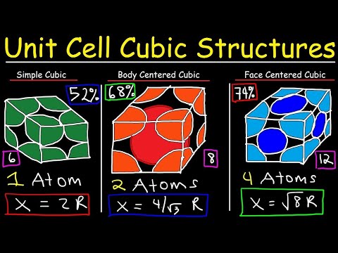
Crystalline solids lie at the opposite end of the “order” spectrum; in a crystalline material, the atoms are arranged in an orderly three-dimensional array. The overwhelming number of devices fabricated today employ crystalline semiconductors.
Polycrystalline materials are also called multicrystalline or polycrystals. They are solids that are composed of many crystallites of varying size and orientation. Crystallites are also referred to as grains. They are small or even microscopic crystals and form during the cooling of many materials. Their orientation can be random with no preferred direction, called random texture, or directed, possibly due to growth and processing conditions.
 0:02:42
How to Understand Crystal Structures?
 0:20:42
The Structure of Crystalline Solids
 0:05:17
Seven Crystal Systems | Trick to remember 7 crystal systems
 0:48:06
18. Introduction to Crystallography (Intro to Solid-State Chemistry)
 0:05:07
How do crystals work? - Graham Baird
 0:17:22
Unit Cell Chemistry Simple Cubic, Body Centered Cubic, Face Centered Cubic Crystal Lattice Structu
 0:00:29
Methods for Determining Atomic Structures: X-ray Crystallography (from PDB-101)
 0:10:54
Lattice Structures in Ionic Solids
 0:22:08
Chemistry of Material Sciences: Understanding the Basics Mini-Lecture (22 Minutes)
 0:13:17
Introduction to Crystal Structures
 1:10:54
Lecture - Intro to Crystallography
 0:14:49
The 7 Crystal Systems!
 0:12:41
What gives crystals different shapes? | The 7 crystal systems
 0:07:02
Introduction to Crystal Structure | Crystal Structure
 0:05:13
Miller indices simplest explaination| animation
 0:32:16
Crystal Structures
 0:07:59
The Composition of Rocks: Mineral Crystallinity and Bonding Types
 0:13:18
Lecture 7 Representing Crystal Structures
 0:03:32
Face Centered Cubic Crystal Structure
 0:10:28
59 The diamond cubic crystal structure
 0:32:01
Understanding Crystal Structures: Symmetry and Lattices Explained
 0:15:31
1.2 Crystal geometry
 0:00:59
Trick to learn seven crystal systems | Najam academy
 0:12:08
Coordination number of Simple cubic, FCC, BCC and hcp lattice
Комментарии