filmov
tv
LVDS Simulation and Measurements on Sigrity Topology Explorer 17.4

Показать описание
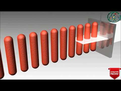
Want to know about LVDS Signaling Simulation and Measurements, what are the different constraints we should simulate in Pre-Layout Analysis, Today I'm sharing the best ways to Simulate LVDS Driver Receiver Model using Sigrity Topology Explorer 17.4
🎥Video Timeline:
○ Section-1 of Video
[00:00] Video Introduction
[00:55] Purpose of doing Pre-Layout Analysis.
[01:25] What are All the Constraints we do Pre-Layout Analysis for.
[02:20] Requirements to Create Realistic Topology
[03:58] Create Topology in Sigrity Topology Explorer and Run the Simulation
○ Section-2 of Video
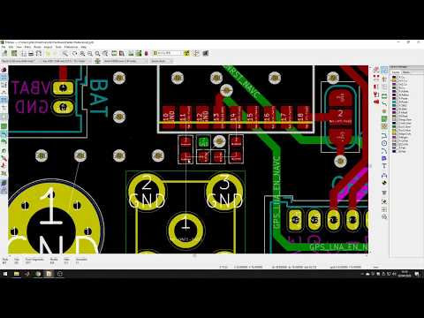
[04:17] Step 1: How to Create a New Topology and Save it.
[04:58] Step-2 Add Driver Block and Assign IBIS model to it.
[06:40] Step-3 Add Receiver Block and Assign IBIS model to it.
[08:14] Step-4 Add Transmission line and Add Stack-up Information
[11:08] Step-5 Connect All the Blocks and Add Termination Resistor at RX
[12:30] Step-6 Set Analysis Options and Stimulus for Driver Side.
[14:20] Step-7 Run the Simulation and Do measurements for Rise/Fall Time, Amplitude, Time Delay etc.
[18:21] Outro
▬▬▬▬▬▬▬▬▬▬▬▬▬▬▬▬▬▬▬▬
✦ Important Cadence Links:
▬▬▬▬▬▬▬▬▬▬▬▬▬▬▬▬▬▬▬▬
Register for your free trial of Cadence Sigrity TopXplorer tool:
Read more about differential signaling and it’s advantages:
▬▬▬▬▬▬▬▬▬▬▬▬▬▬▬▬▬▬▬▬
✦ EsteemPCB Courses on Udemy:
▬▬▬▬▬▬▬▬▬▬▬▬▬▬▬▬▬▬▬▬
✦ Signal and Power Integrity - Simplified: Dr. Eric Bogatin:
▬▬▬▬▬▬▬▬▬▬▬▬▬▬▬▬▬▬▬▬
QUERIES SOLVED
○ LVDS Simulation and Measurements on Sigrity Topology Explorer 17.4
○ What is LVDS Signaling and Working of LVDS
○ How LVDS Works and How to Simulate LVDS
○ What is Low Voltage Signaling Scheme and Simulation of LVDS
○ LVDS Driver Receiver Model
○ What is LVDS Driver and What is LVDS Receiver?
○ LVDS SIMULATION IN TOPOLOGY EXPLORER
○ LVDS Overview and LVDS Simulation in Cadence Orcad
○ Working of LVDS and IBIS Simulations or LVDS IBIS Simulation
○ LVDS Simulation and Measurements
#lvds #simulation #cadence
🎥Video Timeline:
○ Section-1 of Video
[00:00] Video Introduction
[00:55] Purpose of doing Pre-Layout Analysis.
[01:25] What are All the Constraints we do Pre-Layout Analysis for.
[02:20] Requirements to Create Realistic Topology
[03:58] Create Topology in Sigrity Topology Explorer and Run the Simulation
○ Section-2 of Video
[04:17] Step 1: How to Create a New Topology and Save it.
[04:58] Step-2 Add Driver Block and Assign IBIS model to it.
[06:40] Step-3 Add Receiver Block and Assign IBIS model to it.
[08:14] Step-4 Add Transmission line and Add Stack-up Information
[11:08] Step-5 Connect All the Blocks and Add Termination Resistor at RX
[12:30] Step-6 Set Analysis Options and Stimulus for Driver Side.
[14:20] Step-7 Run the Simulation and Do measurements for Rise/Fall Time, Amplitude, Time Delay etc.
[18:21] Outro
▬▬▬▬▬▬▬▬▬▬▬▬▬▬▬▬▬▬▬▬
✦ Important Cadence Links:
▬▬▬▬▬▬▬▬▬▬▬▬▬▬▬▬▬▬▬▬
Register for your free trial of Cadence Sigrity TopXplorer tool:
Read more about differential signaling and it’s advantages:
▬▬▬▬▬▬▬▬▬▬▬▬▬▬▬▬▬▬▬▬
✦ EsteemPCB Courses on Udemy:
▬▬▬▬▬▬▬▬▬▬▬▬▬▬▬▬▬▬▬▬
✦ Signal and Power Integrity - Simplified: Dr. Eric Bogatin:
▬▬▬▬▬▬▬▬▬▬▬▬▬▬▬▬▬▬▬▬
QUERIES SOLVED
○ LVDS Simulation and Measurements on Sigrity Topology Explorer 17.4
○ What is LVDS Signaling and Working of LVDS
○ How LVDS Works and How to Simulate LVDS
○ What is Low Voltage Signaling Scheme and Simulation of LVDS
○ LVDS Driver Receiver Model
○ What is LVDS Driver and What is LVDS Receiver?
○ LVDS SIMULATION IN TOPOLOGY EXPLORER
○ LVDS Overview and LVDS Simulation in Cadence Orcad
○ Working of LVDS and IBIS Simulations or LVDS IBIS Simulation
○ LVDS Simulation and Measurements
#lvds #simulation #cadence
 0:18:42
LVDS Simulation and Measurements on Sigrity Topology Explorer 17.4
 0:13:30
What is LVDS Signaling Scheme? Working of LVDS and IBIS Simulations
 0:06:51
What is LVDS?
 0:04:19
What is multidrop LVDS?
 0:01:38
Electronics: How to connect LVDS signals to oscilloscope?
 0:04:00
Why is 50 OHM impedance used in PCB Layout? | Explained | Eric Bogatin | #HighlightsRF
 0:02:25
Electronics: Convert single-ended (analog) signal to LVDS
 0:03:39
Differential- and Common mode
 0:02:28
How is LCD Working? An animated video
 0:06:25
How to add external hysterisis to a high speed LVDS comparator
 0:15:44
Differential Signaling: Designing for Long, Fast, or Noisy Applications
 0:47:50
Optimised M-LVDS Solutions for High-Density Systems
 0:02:13
How to Properly Terminate a Clock Signal by Identifying Common Signal Integrity Issues
 0:02:13
Electronics: Difference between LVPECL and PECL (2 Solutions!!)
 0:14:11
Impedance Measurements Using Altium Designer's Signal Integrity Tool
 0:07:17
Waveform Measurement on HyperLynx Oscilloscope | High-Speed Simulation Tutorial-3
 0:43:57
Signal Integrity for High Speed Design
 0:00:46
NEVER buy from the Dark Web.. #shorts
 0:03:57
Intro to Differential Signaling Technologies and Devices
 0:04:48
Introduction of DC SCM 2 0 LVDS Tunneling Protocol & Interface LTPI
 0:12:01
KiCad Controlled Impedance Traces (e.g. 50Ω) - Phil's Lab #3
 0:22:22
Design Example: Wolfspeed MMIC Design
 0:10:06
EMI Control with Hot Digital, Low Level Analog Long, Leads & Plastic Box
 0:11:25
CAN Bus: Serial Communication - How It Works?
Комментарии