filmov
tv
The next step in nanotechnology | George Tulevski

Показать описание
Nearly every other year the transistors that power silicon computer chip shrink in size by half and double in performance, enabling our devices to become more mobile and accessible. But what happens when these components can't get any smaller? George Tulevski researches the unseen and untapped world of nanomaterials. His current work: developing chemical processes to compel billions of carbon nanotubes to assemble themselves into the patterns needed to build circuits, much the same way natural organisms build intricate, diverse and elegant structures. Could they hold the secret to the next generation of computing?
TEDTalks is a daily video podcast of the best talks and performances from the TED Conference, where the world's leading thinkers and doers give the talk of their lives in 18 minutes (or less). Look for talks on Technology, Entertainment and Design -- plus science, business, global issues, the arts and much more.
TEDTalks is a daily video podcast of the best talks and performances from the TED Conference, where the world's leading thinkers and doers give the talk of their lives in 18 minutes (or less). Look for talks on Technology, Entertainment and Design -- plus science, business, global issues, the arts and much more.
 0:09:36
The next step in nanotechnology | George Tulevski
 0:04:42
What is nanotechnology?
 0:11:44
Nanotechnology is not simply about making things smaller | Noushin Nasiri | TEDxMacquarieUniversity
 0:04:27
The Next Step in Nanotechnology ( George Tulevski) by TED Talks
 0:00:37
The Next Step in Nanotechnology #nanotechnology #nano #technology
 0:00:44
How Can the Next Step in Nanotechnology Impact My Future?
 0:07:13
What is Nanotechnology ?The next step in nanotechnology |
 0:24:00
Nanotechnology Expert Explains One Concept in 5 Levels of Difficulty | WIRED
 0:58:06
114 Academic Words Ref from 'George Tulevski: The next step in nanotechnology | TED Talk'
 0:30:50
Applications of Nanoscience and Nanotechnology
 0:13:22
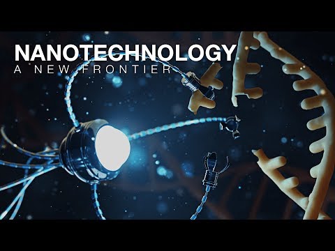
Nanotechnology: A New Frontier
 0:54:25
NACK - What is Nanotechnology?/How Small is a Nanometer?
 0:52:23
Nanotechnology: The High-Tech Revolution - with Dave Blank
 0:41:36
Nanotechnology Documentary
 0:48:48
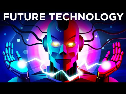
20 Emerging Technologies That Will Change The World
 0:16:22
Nanoscience and drug delivery -- small particles for big problems | Taylor Mabe | TEDxGreensboro
 0:11:52
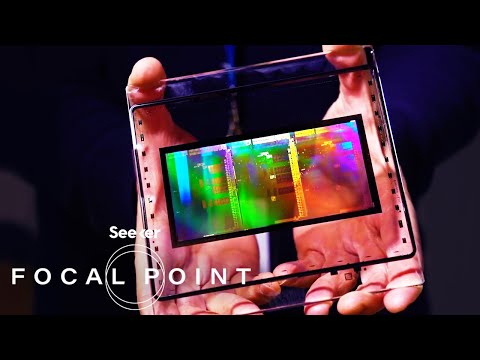
The Extreme Physics Pushing Moore’s Law to the Next Level
 0:11:13
Timelapse of Future Technology: Next 1000 Years
 1:17:10
Accelerating Research in Applied Nanotechnology
 0:02:47
7 Amazing Everyday Examples Of Nanotechnology In Action
 0:18:49
Bio Nano Technology-New Frontiers in Molecular Engineering: Andreas Mershin at TEDxAthens
 0:00:40
Nanotechnology in Electronics: Advancements and Potential
 0:03:35
Basic terms in Nanotechnology
 1:02:25
Nanotechnology’s Promise: A Big Risk in a Small Package?
Комментарии