filmov
tv
The Path to 1,000-Layer 3D NAND

Показать описание
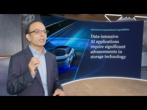
For decades, Lam Research has been a leading provider of manufacturing equipment solutions that advance vertical, lateral, and logical scaling in semiconductor devices. Today, artificial intelligence is driving the development of the most complex chips ever built. As we navigate the complexities of the AI era, the path to 1000-layer 3D NAND represents more than just a technological advancement; it symbolizes a leap toward meeting future data demands. Hear from Harmeet Singh, GVP and GM of Lam’s Etch Product Group, about what comes next on the journey to 1000 layers.
Social Media:
Social Media:
 0:14:00
The Path to 1,000-Layer 3D NAND
 0:00:11
This video makes you feel trypophobia 🐝😩 #sfx #sfx_makeup #youtubeshorts #makeup #shorts
 0:00:41
Will water make it FASTER? 🤔
 0:00:24
Walking tree caught moving😳 #shorts
 0:00:12
which one is drawing 🙈
 0:00:48
Aliens👽
 0:00:08
Asteroid Hitting The Moon🌒💥#lunarsurface #telescope #moon #asteroid #nasa #space #shorts
 0:00:13
Armors in RPG games be like
 0:00:08
MY EYEBALL POPPED OUT 😳
 0:00:13
I broke my PS5 controller because of my step sis #shorts
 0:00:10
Minecraft Villager Stop Motion 😬 #Shorts
 0:00:13
Sun Damage Is Terrifying
 0:00:19
When You Buy a New Weapon in an RPG
 0:00:17
Liver Cancer Symptoms That are Often Overlooked
 0:00:06
xavier memes #memes
 0:00:10
Skydiving with NO PARACHUTE 😂
 0:00:13
Queen cake 🍰 #cakeanything #laramason
 0:00:11
Why did this happen to me (Rubik's Cube FAIL)
 0:38:13
Pre-Historic Underground Mega-Complex Discovered in Egypt
 0:00:37
I couldn’t pull out 🥵
 0:00:33
What Is A Tapeworm? 😨
 0:00:27
The Only Three Ways You Should Add Blood To LEGO Minifigures #shorts
 0:00:10
What I imagine when I hear this OST
 0:28:34
DIY Arduino Automatic Domino Layer - 3D Printing & Assembly - Elegoo
Комментарии