filmov
tv
KiCad Ground Planes Tutorial (1m)

Показать описание
NOTE 1: I should have mentioned in the video that you can force recalculation of these polygons using the "B" key (or whatever shortcut you have configured)
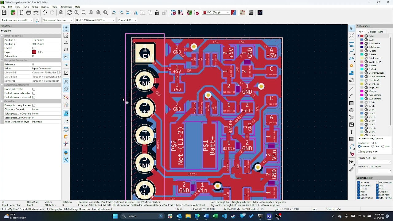
NOTE 2: In the video I was very careful to match the outline of the board. This is not necessary. KCcad is smart enough such that you can simply cover the entire area with a polygon and it will only fill the areas that are actually inside the board! This is especially useful if you're making boards with weird shapes.
A ground plane is a large area of copper on a printed circuit board (PCB) that is connected to the ground signal. The purpose of a ground plane is to provide a low-impedance path for ground signals and to shield the signal traces from interference. Ground planes can also help to improve signal integrity, reduce EMI/RFI, and increase the overall performance of the circuit. Ground planes are particularly useful in high-speed and high-frequency applications, where signal integrity is critical, as they can help to reduce signal reflection and crosstalk. It is also common to have planes for other power signals (e.g., 3.3V) on the inner layers of the board for similar reasons as well as to simplify the overall routing of the wires.
KiCad Ground Planes Tutorial (1m)
KiCad 6: Ground Plane (Filled Zone)
#1421 PCB - Grounds
kicad ground plane
H Bridge PCB Layout in 30 seconds using Kicad
Received PCB From Various Manufacturers - KiCad 7 tutorial series #pcb #electronics
KiCad PCB Shape from DXF Tutorial (1m)
KiCad 7 Tutorial: Buses (Part 7)
Routing over Split Ground Plane? - One Minute #PCBDesign Review 09 #electronics #altium
Adding Copper Plane in KiCad
Add Groundplane to a Kicad 6 0 PCB
How and When to Use Ground Fills
KiCad v5.99: convert circle to copper zone keep-out
Electronics: Why isn't my ground plane in Kicad connecting all of my grounds? (2 Solutions!!)
Getting Started with KiCAD - PART 6 - Net labels
Tame the yellow line: Master KiCad 7 Edge.Cuts
Using Ground Copper in KiCAD
8051 Mini Development Board PCB Design in KiCAD
Getting Started with KiCAD - PART 5 - Power rails
How to Ground Plane in Autodesk Eagle using Polygon | Autodesk Eagle Tutorial
kicad tutorial beginners
Ground GND #pcb ⚡🕹️🎥🎮💻🔌💡🤖
[KiCad] Cara Membuat Ground Plane Pada KiCad 5 | Part 6 - VLOG16
Dual Power Supply PCB Design in KiCAD
Комментарии
 0:01:21
 0:01:31
 0:11:32
 0:12:37
 0:00:31
 0:00:08
 0:01:25
 0:03:56
 0:01:00
 0:07:31
 0:05:04
 0:03:30
 0:00:19
 0:03:01
 0:00:23
 0:05:50
 0:06:43
 0:00:21
 0:00:49
 0:00:17
 0:00:15
 0:00:16
![[KiCad] Cara Membuat](https://i.ytimg.com/vi/qw8K4m7PiKI/hqdefault.jpg) 0:04:39
0:04:39
 0:00:21