filmov
tv
Common Emitter (CE) Transistor Configuration in tamil

Показать описание
Transistor Common Emitter (CE) Configuration. Definition:
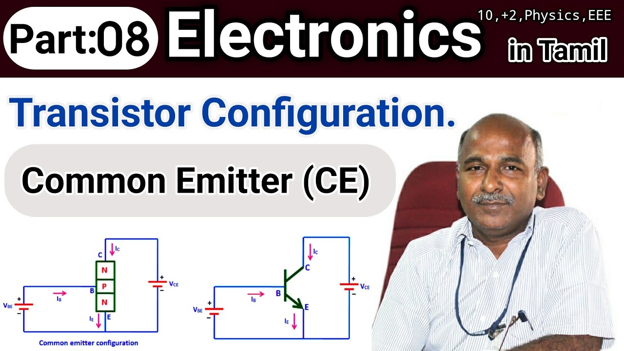
The configuration in which the emitter is connected between the collector and base is known as a common emitter configuration. The input circuit is connected between emitter and base, and the output circuit is taken from the collector and emitter. Thus, the emitter is common to both the input and the output circuit, and hence the name is the common emitter configuration. The common emitter arrangement for NPN and PNP transistor.
Base Current Amplification Factor (β)
The base current amplification factor is defined as the ratio of the output and input current in a common emitter configuration. In common emitter amplification, the output current is the collector current IC, and the input current is the base current IB.
In other words, the ratio of change in collector current with respect to base current is known as the base amplification factor. It is represented by β (beta).
Common Emitter Configuration
In common emitter configuration, base is the input terminal, collector is the output terminal and emitter is the common terminal for both input and output. That means the base terminal and common emitter terminal are known as input terminals whereas collector terminal and common emitter terminal are known as output terminals.
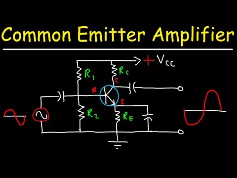
In common emitter configuration, the emitter terminal is grounded so the common emitter configuration is also known as grounded emitter configuration. Sometimes common emitter configuration is also referred to as CE configuration, common emitter amplifier, or CE amplifier. The common emitter (CE) configuration is the most widely used transistor configuration.
The common emitter (CE) amplifiers are used when large current gain is needed.
The input signal is applied between the base and emitter terminals while the output signal is taken between the collector and emitter terminals. Thus, the emitter terminal of a transistor is common for both input and output and hence it is named as common emitter configuration.
The supply voltage between base and emitter is denoted by VBE while the supply voltage between collector and emitter is denoted by VCE.
In common emitter (CE) configuration, input current or base current is denoted by IB and output current or collector current is denoted by IC.
The common emitter amplifier has medium input and output impedance levels. So the current gain and voltage gain of the common emitter amplifier is medium. However, the power gain is high.
To fully describe the behavior of a transistor with CE configuration, we need two set of characteristics – input characteristics and output characteristics.
Input characteristics
The input characteristics describe the relationship between input current or base current (IB) and input voltage or base-emitter voltage (VBE).
First, draw a vertical line and a horizontal line. The vertical line represents y-axis and horizontal line represents x-axis. The input current or base current (IB) is taken along y-axis (vertical line) and the input voltage (VBE) is taken along x-axis (horizontal line).
To determine the input characteristics, the output voltage VCE is kept constant at zero volts and the input voltage VBE is increased from zero volts to different voltage levels. For each voltage level of input voltage (VBE), the corresponding input current (IB) is recorded.
Thank you for watching
Комментарии
 0:13:12
 0:11:25
 0:05:23
 0:08:58
 0:09:28
 0:01:00
 0:33:29
 0:02:47
 0:04:55
 0:06:31
 0:22:59
 0:07:05
 0:07:56
 0:11:09
 0:06:04
 0:00:13
 0:06:39
 0:00:11
 0:00:28
 0:21:36
 0:13:48
 0:00:06
 0:22:31
 0:21:17