filmov
tv
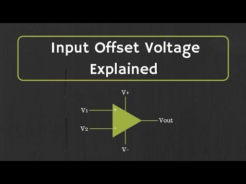
Non-Ideal Op Amps: Input Offset Voltage

Показать описание
Input offset voltage is one of the non-ideal characteristics of an op amp. It can be modeled as a small voltage source in series with one of the input terminals of the op amp. Input offset voltage is an unavoidable property because it is due to the semiconductor manufacturing process. It can be compensated for either through modifications to the external circuit or by adding compensation inside the op amp during manufacturing.
This video explains what input offset voltage is, how it effects various op amp circuits, and different ways to compensate for it.
To see more about operational amplifier check out:
To see more content related to electrical and electronic circuits, check out:
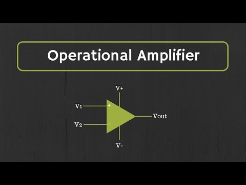
This video explains what input offset voltage is, how it effects various op amp circuits, and different ways to compensate for it.
To see more about operational amplifier check out:
To see more content related to electrical and electronic circuits, check out:
 0:11:14
Non-Ideal Op Amps: Input Offset Voltage
 0:12:02
Operational Amplifiers - Inverting & Non Inverting Op-Amps
 0:11:39
Op-Amp: Input Offset Voltage Explained
 0:07:12
Non-Ideal Operational Amplifier 1: Part 1
 0:13:32
Non-Idealities of Operational Amplifiers (OpAmps)
 0:06:18
Non Ideal Vs Ideal Op Amp Circuit
 0:09:50
Non-Ideal Op Amps: Input Bias Current
 0:08:53
DC Imperfections (Theory)
 0:11:28
PEO solved examples (ELEC A5): Non-Ideal OP AMP Questions no. 3 & 4
 0:13:59
Problem 9: Non-Ideal Op Amp
 0:49:32
EEVblog #600 - OpAmps Tutorial - What is an Operational Amplifier?
 0:16:21
ECE3400 Lecture 37: Non-Ideal Op Amps: Non-Inverting Configuration (Analog Electronics)
 0:15:09
Intro to Op-Amps (Operational Amplifiers) | Basic Circuits
 0:14:41
Non ideal op amp example question
 0:34:42
15 DC Imperfections
 0:00:09
How Op Amp Non Inverting Amplifier Work In Electronics Circuit
 0:13:10
Introduction to Operational Amplifier: Characteristics of Ideal Op-Amp
 0:07:48
Input Bias Current in Op-Amps (Amplifiers #9)
 0:04:19
Op Amp Gain | Details Calculations Formulas
 0:05:45
#890 Basic: Op-Amp Offset (when zero is not zero)
 0:16:01
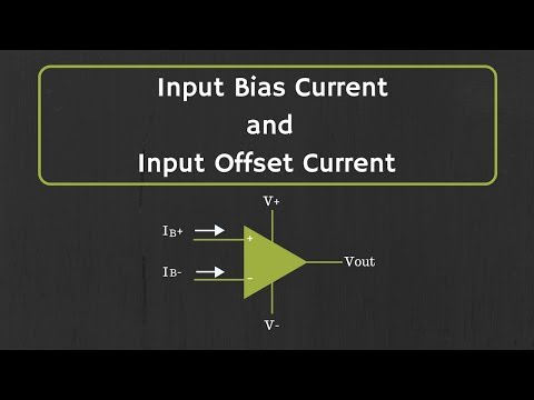
Op-Amp: Input Bias Current and Input Offset Current Explained
 0:03:10
Non-Ideal Op-Amps
 0:04:10
10. Input Offset Voltages
 0:34:14
EEVblog #479 - Opamp Input Bias Current
Комментарии