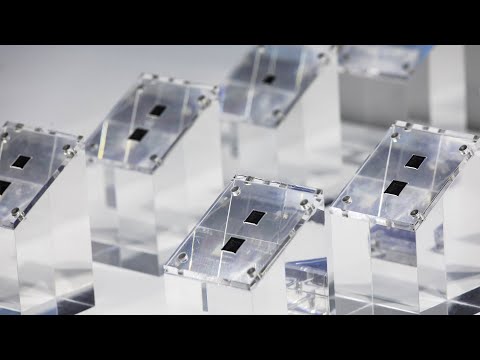
Bigger Chips = Better AI? Nvidia's Blackwell vs. Cerebras Wafer Scale Engine

preview_player
Показать описание

Nvidia's new Blackwell GPU is HUGE, literally! If you’re looking to be an Nvidia AI chip competitor, why not just make physically bigger chips? In this video, we explore the physics and economics behind AI chip design. We'll cover Nvidia's Blackwell packaging secrets, rival Cerebras Systems' wafer-scale chips, and the critical role of fab equipment makers in the race for AI system dominance.

Other vids to check out:

**************************************************************************************
Affiliate links that are sprinkled in throughout this video. If something catches your eye and you decide to buy it, we might earn a little coffee money. Thanks for helping us (Kasey) fuel our caffeine addiction!

Chapters:
00:00 Introduction to Megachips: Why It's Not Simple
00:29 Exploring NVIDIA's Blackwell GPU and Cerebras' Monster Chip
01:22 Diving Deep into Chip Manufacturing Challenges
03:53 Advanced Packaging Techniques: Chiplets and Heterogeneous Integration
10:25 Cerebras' Wafer Scale Engine: A Game Changer?
12:13 The Five Major Challenges of Megachip Manufacturing
16:41 Economic Constraints and the Future of Chip Manufacturing
18:44 Investment Opportunities in the Semiconductor Industry

Content in this video is for general information or entertainment only and is not specific or individual investment advice. Forecasts and information presented may not develop as predicted and there is no guarantee any strategies presented will be successful. All investing involves risk, and you could lose some or all of your principal.

#cerebras #nvidia #semiconductors #chips #investing #stocks #finance #financeeducation #silicon #artificialintelligence #ai #financeeducation #chipstocks #finance #stocks #investing #investor #financeeducation #stockmarket #chipstockinvestor #fablesschipdesign #chipmanufacturing #semiconductormanufacturing #semiconductorstocks

Nick and Kasey own shares of Nvidia, Cadence Design Systems, AMD, and Synopsys
Рекомендации по теме
Комментарии
Автор

👉👉Want more Chip Stock Investor? Our membership delivers exclusive perks! Join our Discord community, get downloadable show notes, custom emojis, and more. Become a true insider – upgrade your experience today!

chipstockinvestor
Автор

REQUEST: an episode of details of most important NVIDIA "partnerships" and what it means for the company's future. You guys are awesome.

alexsassanimd
Автор

Cerebras pace of making smaller and smaller transistors in large scale wafers, suggests they have some systematic understanding of how to deal with the thermal/quantum jitters. ASML now has 1 nm feature size ability(ASML's technology is also a technological miracle. And, they can see how they can go beyond their current miracle. ). So, I expect Cerebras for one to beat their cs-3

oker
Автор

NVidia makes its chips at or near the retical limit, as does WSE. Both designs overprovision functional units that can be fused off/routed around and still meet the specification (some estimate about 10-20% of H100 chip is disabled silicon).

Nvidia can bin bad chips into lower blackwell products to offset costs, WSE doesn't have this option.


WSE requires a complex cooling system but a lot less networking. Blackwell requires an additional NVlink chip per 8 gpus or so, advanced packaging for the GPU dies/HBM, advanced melanox networking to get a lot of gpus to communicate. So it isn't so clear who wins on a cost basis.

Cerebras seems to have solved the cooling/mechanical problems so in theory they can outperform blackwell on certain models that fit within the chips memory. However that is substantially less memory than blackwell.

darrell
Автор

Good video, but hope video can elaborate more on how Cerebras has solved problems (3) and (4) in their product. And for problem (5), power consumption, although larger chip would consume more power per chip, but it consumes less power for the equivalent compute (of smaller chips stitches together with interconnects or other methods).

kualakevin
Автор

Excellent! As always you both are great teachers in this field! Keep up your amazing hard work! ❤

sugavanamprabhakaran
Автор

Very interesting video, especially the five reasons for size limiations at the end. #1 was new and interesting to me. But it makes sense. This is something most non-experts would probably not find out by themselves easily. #2 was relatively obvious. Carebras has at least somehwhat of a solution for this as you mentioned. They are somehow routing around damaged transistors (not sure how effective their solution is). #3 also makes sense. But like with #1 most people wouldn't know by how much exactly this would limit the chip size. #4 also makes sense. Maybe materials science could help here!? or maybe the optimal available materials are already used. It would seem that Nvidia wouldn't make compromises here given the product price. #5 I guess the previous points all play into this TCO calculation and it is probably cheaper to cool separate smaller chips. It would be interesting to know if the Nivida CEO thinks that the size of the Blackwell chips is already optimal or if it could make sense to grow chip size further at least for very large customers who need the most computing power. I asked Gemini why 300 mm is the current standard for wafers. One interesting aspect is that precisely handling 450 mm diameters wafers for example would be an immense technological challenge, because the wafers are so fragile.

valueinvestor
Автор

Nice to discover a video of NotebookLM’s previous model. It was definitely less life like and realistic than today.

matteoianni
Автор

I found interesting book: "Chiplet Design and Heterogeneous Integration Packaging" by by John H. Lau. 895 pages. The book focuses on the design, materials, process, fabrication, and reliability of chiplet design and heterogeneous integraton packaging. Both principles and engineering practice have been addressed, with more weight placed on engineering practice. This is achieved by providing in-depth study on a number of major topics such as chip partitioning, chip splitting, multiple system and heterogeneous integration with TSV-interposers, multiple system and heterogeneous integration with TSV-less interposers, chiplets lateral communication, system-in-package, fan-out wafer/panel-level packaging, and various Cu-Cu hybrid bonding. The book can benefit researchers, engineers, and graduate students in fields of electrical engineering, mechanical engineering, materials sciences, and industry engineering, etc.

Stan_
Автор

Great video. Good basic explanation regarding the 5 main reasons chips cannot easily be made bigger.👍

majidsiddiqui
Автор

Another plethora of important info....thanks as always

mdo
Автор

HIGH QUALITY CONTENT!!! the 5 reasons on chips size limits was excellent... love it!

rastarebel
Автор

Your channel has come to my eyes at the right time...but I wished I knew this channel before the AI frenzy 2 months ago..

eversunnyguy
Автор

Excellent presentation. Thanks for sharing….

zebbie
Автор

The entire wafer is etched by reticles before it's cut into chips, so I don't see how problem #1, 'the reticle" is a problem for using the entire wafer for 1 chip. As for defects, the architecture enables bypassing sections that have a defect. Groq does this. It's not simply "infrastructure" that limits wafers to 12 inches, but the inability to make the flow of gases and heat across the entire wafer perfectly even. You could slow each step down to help gases and heat spread more evenly, but that reduces production rate. The only very fundamental physics problem is that you want as much of the chip to be synchronized with the clock steps as much possible because parallel computing for generalized algorithms can greatly waste computation. You can't have the entire wafer synch at high clock speeds because, for example, at 1 GHz, light can travel only 300 mm and it's not a straight path across the chip & capacitances greatly reduce that max speed, and at 1 GHz you really need everything sync'd at less than 1/4 the clock cycle (75 mm max distance). Fortunately, video and matrix multiplication are algorithms that can efficiently do parallel ("non-sync'd") computation. Training can't do parallel efficiently, but inference can, although NVDA's GPU architecture can't do it nearly as efficient as theoretically possible. Groq capitalizes on this, not needing any switches (Jensen was proud of NVDA's new switches being more efficient) or any L2 or cache (which at least 2x the energy per compute required), which is why Groq is 10x more tokens per energy than H100.

heelspurs
Автор

Thanks Crew. I wonder if you might do a video on Brainchip Corps neuromorphic Akida chip ? I'm very curious to understand how the Akida 2000 works because it has memory embedded in the chip in 4 memory configurations to a 'node' or an axiom. Producing a super low powered chip. I'm wondering why other companies aren't following this design? And does it have the potential to be scaled into training ?

styx
Автор

Great content ! I learned a lot from it,

Stan_
Автор

Nvidia has the fastest interconnect of all the competitors ... Nvidia also is the company that started all of this, really with Deep learning! Plus, Nvidia is more than capable of making a wafer scale chip if the believed it was a better Nvidia also has the Best software stack and tools for the

chrisgarner
Автор

Bigger chip = higher defect rate. If the chip is designed to deal with failed parts of the die so they can still get to market (pathways through the chip can be disabled and the chip specs allow for a certain percentage of the chip to fail in production), then it's not terrible. But a wafer size chip is a nightmare.

Pretty much any wafer that comes off a line has defects. It's only a matter of percentage. The prevailing knowledge is that the smaller you can make a die (chip), the smaller the percentage will be for chips that fail off that one wafer. For instance is a single wafer is used to make ONE chip AND there is no allowance for failed parts of that chip, then the failure rate is pretty much always going to be 100% and of course that's not feasible.

johndoh
Автор

GREAT video! I can't believe you continue to produce such great content. Job well done, and a BIG thanks!!

shannonoliver