filmov
tv
EP4 – DIY PCB – Laser Etching Experiments

Показать описание
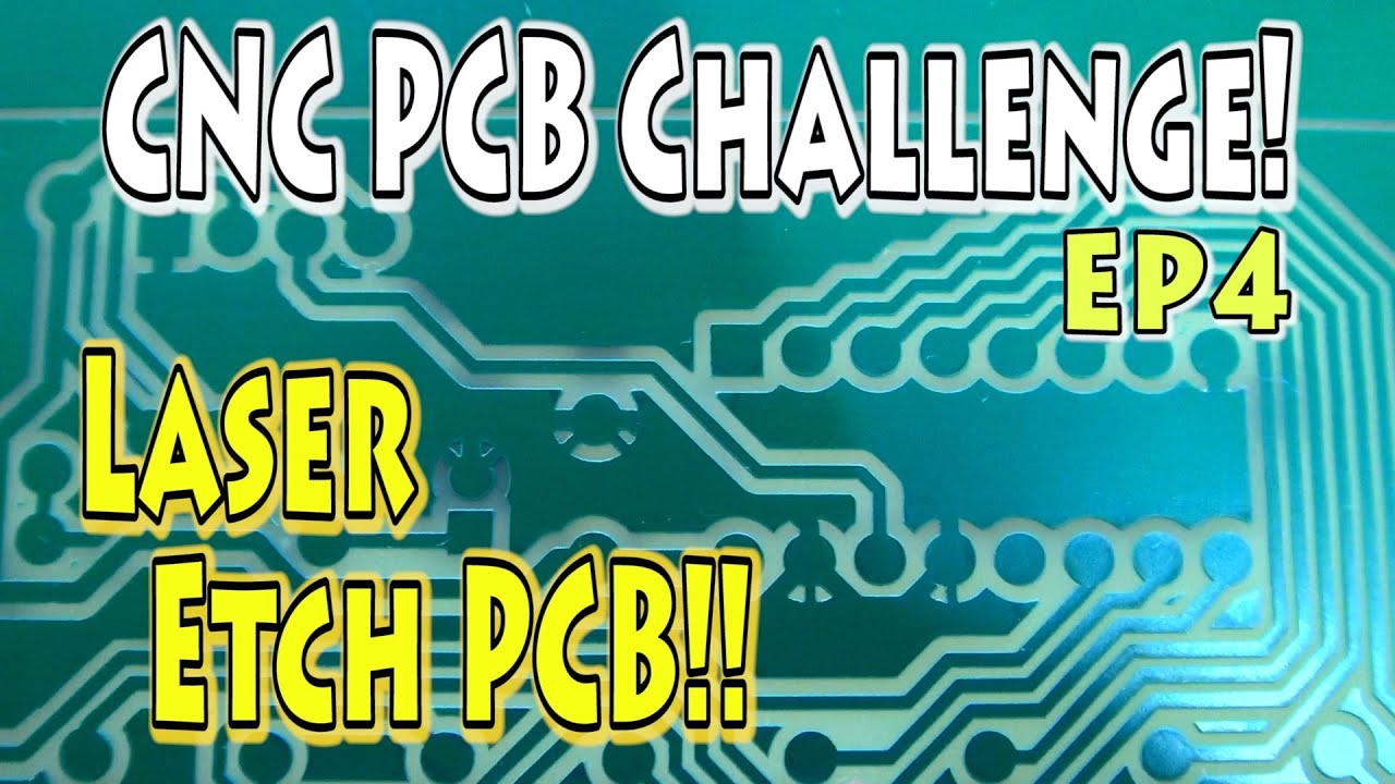
Lots of experimenting in this episode, as I switch things up, and look using a etch based solution, with the CNC’s laser being used to create the etch resist pattern.
My current plan is to try use the CNC’s laser where ever possible, as I believe this will provide the most accurate and consistent result.
This is the fourth episode in a series where I am challenging myself to make the best possible DIY PCB’s using commonly available low cost CNC technologies.
My current plan is to try use the CNC’s laser where ever possible, as I believe this will provide the most accurate and consistent result.
This is the fourth episode in a series where I am challenging myself to make the best possible DIY PCB’s using commonly available low cost CNC technologies.
EP4 – DIY PCB – Laser Etching Experiments
How to Make a PCB | ep 4 | Ordering Your PCB!
DIY PCB Design - Episode 4 - PCB Schematic Designing
Convert Project Circuit into PCB | PCB Designing Tutorial EP:4
PCB Journey Episode 4, Lamination
PCB Design - Understanding Datasheets - Drawing Schematics - Altium - Making a Robot Arm - EP4 - FWE
PCB Design & 3D Printer - How To Make A Product Episode 4
Schematic Design - Landing Model Rockets Ep. 4
How to Solder Your First Circuit, Soldering/Desoldering/Heat Rework Tutorial THC & SMD
EP5 – DIY PCB – Single Sided PCB made with CNC3018
DIY Computer Upgrade: Can We Install a Replica Keyboard PCB? Ep 4
Father & Sonthesizer Ep.4: Making a PCB
Eurorack DIY: 909 Rimshot (Episode 4) - Routing the PCB
Using isopropyl alcohol to find a faulty part on a PCB
Clean BATTERY CORROSION on ELECTRONICS! EASY DIY! | 2-minute Tutorials Ep.4
Ardumower PCB 1.4 Episode 4 - Soldering sockets for Arduino Due
EP7 – DIY PCB – Best DIY PCB EVER! (Double Sided SMD)
ESP32C3 Smart door sensor #iot #electronics #engineering #pcb #design #pcba #soldering #diy #esp
EP3 – DIY PCB – CNC Milling a PCB
How To Clean Water Damage pcb
SWITCHES - The Secret Life of Components, a series of guides for designers and makers - Episode 4
3D Printing Basics: Parts names, care, and filament types! (Ep4)
EP8 – DIY PCB – Corner Probe for CNC3018 (Contactless)
DIY Keyboard Ep.4 - Software
Комментарии
 0:23:36
 0:07:35
 0:08:02
 0:15:38
 0:03:22
 0:52:34
 0:06:00
 0:58:54
 0:38:50
 0:16:35
 0:30:25
 0:11:22
 0:27:34
 0:00:12
 0:02:04
 0:20:47
 0:26:31
 0:00:20
 0:25:21
 0:00:49
 0:32:31
 0:18:25
 0:28:18
 0:34:50