filmov
tv
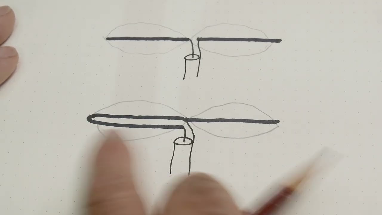
#1456 PCB Yagi antenna for 2.4GHz
Показать описание
Episode 1456
I bought this off eBay. Let's test it.
I bought this off eBay. Let's test it.
 0:15:49
#1456 PCB Yagi antenna for 2.4GHz
 0:00:06
Original PCB flat panel antenna
 0:00:16
Yagi 3 elements Antenna for basement or no cellular signal area's
 0:00:08
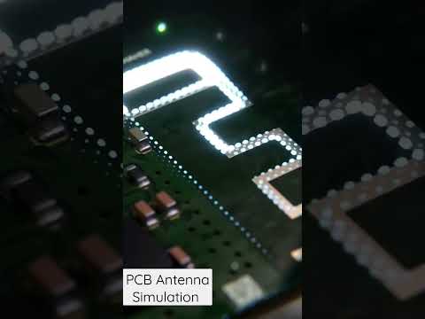
PCB Antenna Simulation in Blender and openEMS #blender3d #b3d #electronics #antenna #simulation
 0:14:05
#1459 PCB Yagi antenna for 2.45GHz (part 1 of 2)
 0:02:04
#1460 PCB Yagi antenna for 2.45GHz (part 2 of 2)
 0:25:24
A Simple PCB 2 4GHz Wifi Yagi
 0:00:18
printed yagi uda antenna 0.8GHz to 6GHz bandwidth using CST
 0:09:40
#1469 2.45 GHz Yagi A Good One!
 0:07:42
#1521 YAGI design for 2.45 GHz (part 1 of 3)
 0:00:11
printed yagi uda antenna array of dipoles operating at 0.8GHz,0.9GHz,2.4GHz,3.8GHz,5.8GHz in hfss
 0:02:15
Test 5-el Yagi na 13 cm (2.4GHz)
 0:00:29
PCB Antenna
 0:01:48
Mini test reception : 1/4 Lambda vertical vs Yagi antenna - FRANCAIS / ENGLISH
 0:00:55
KM5PO 47 GHz rover testing part 2 #ghz
 0:03:11
Unboxing BLUE BEAM ULTRA 1.3GHZ ANTENNA for Long Range FPV Rc Car
 0:00:14
Anti drone PCB antenna
 0:20:07
Rapid Prototyping of a Yagi Antenna
 0:00:48
What is a Cross Yagi?
 0:03:44
How to legally get a massive boost to your WiFi For Under $10
 0:03:42
How to make dipole antenna for transmitter 2.4GHz
 0:00:15
Inside 2.4 ghz antenna
 0:00:24
yagi uda array antenna in cst
 0:00:35
dual band monopole antenna operating at 0.8GHz,0.9GHz,2.4GHz,3.8GHz,5.8GHz in hfss
Комментарии