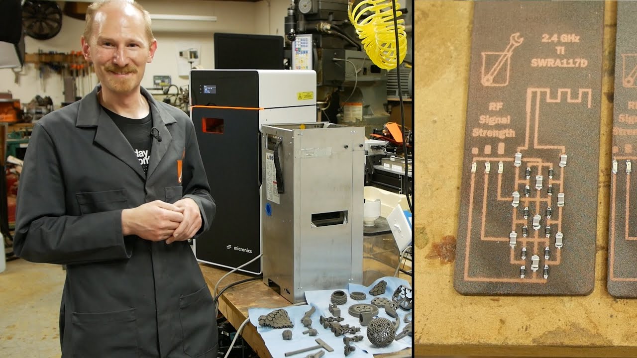
Micronics SLS nylon 3D printer makes electronic circuits
preview_player
Показать описание


Favorite copper plating bath recipe:
Heat 250ml deionized water to 60*C in a 300ml beaker, stirring at 350 RPM
Add 2.5g CuSO4*5H2O, wait until dissolved
Add 4.6g EDTA disodium dihydrate, wait until dissolved
Add 0.84ml of 1% Triton-X 100 solution in water
Dissolve 5.8g NaOH in 30ml DI water, stir until clear, then add to bath
Add 4ml Formaldehyde (37% HCHO)
Lower stirring to 100 RPM and begin filtration with 0.5 micron syringe filter and peristaltic pump. No intentional oxygenation or bubbling. Filter return is below surface for minimal splashing.

I experimented a little with PEG and 2 2' Bipyridine, but didn't find them impactful enough to discuss in this video.

LED rectenna designs:

Electroless copper references:

Copper chromite catalyst:

Open Sauce 2024:

Support Applied Science on Patreon:
Рекомендации по теме
Комментарии
Автор

Did you see strange parts video about this 3d printer? what is your experience? he had a lot of trouble and in the end said he does not think this printer should be sold as soon as the company wants (iirc)

Falqun
Автор

So awesome. Incorporating the pulse laser into the printing process for activation per layer is such a fantastic idea.

funnymyth
Автор

See you at Open Sauce - been a long time!

mikeselectricstuff
Автор

Dude holy shit. I spent like 6 months trying to come up with an electroless copper recipe because I encountered the same issues of non-specificity on all the information and eventually gave up after smashing my head against the wall with so many failures. You are my hero for posting this. I cant wait to give it a go again. Thank you thank you thank you!

ferriswhitehouse
Автор

3d printing metal inside structures could be interesting for making weird antennas

mikeselectricstuff
Автор

Nice! As for printing on 3D surfaces, you might want to look into "aerosol jet printing". This allows the printing on any kind of curved surface with fairly high resolution. BTW, the printing of internal conductive traces is well known in ceramic part manufacture where they generally use silver/ceramic mixtures to create the conductive traces. These parts are then sintered in vacuum. Using this method you can even print passive parts like inductors, resistors and capacitors inside the ceramic.

HuygensOptics
Автор

Focusing a laser projector "by ear"!? That would certainly not have occurred to me, but it makes good sense once you explain it!

JonPMeyer
Автор

A couple of points about the dichroic mirror to make your life easier:
-reflect the shorter wavelength and transmit the longer one (this should be already the default for your set-up)
-if possible (or economically viable), try to find a 1064 Nd:YAG laser for the activation: it will be hard to find a mirror able to split 447nm from 532nm(I guess that's your green laser) and sustain the two lasers power. Most of the dichroic mirrors on the market are designed for fluorescent microscopy.
-if possible, use polarised light: p for the one to be reflected, s for the one to be transmitted
-remember to add an antireflective coating on the back of the mirror, or you will start carving the side of your printer

Lastly, a plate mirror may introduce beam deviations and a tilt in the focal plane of the activation laser; on the other hand, a cube beamsplitter may interfere with the calibration of the printer laset.

Beregorn
Автор

Did not expect this channel to be a part of this Micronics embargo that flooded my feed today but couldn’t be more grateful

Rushil
Автор

This could make some great RF metamaterials.

sumguysr
Автор

It would definitely be cool to see a video specifically proving the idea of printing traces in areas that later aren't optically accessible.

jeremyjedynak
Автор

A company that just sells the product instead of requiring client interrogation first is indeed rare.

TimLF
Автор

I used to run a Shipley 3000 PTH line, and we were adding a 500-1000ml of formaldehyde to the electroless (150 litre) bath every 3-4 hours to keep the plating thickness uniform throughout a production day.

proluxelectronics
Автор

I was working on 3D printed electronics in my phd. At the begining I had similar idea that you presented in 16:20, but my problem was achieving copper in the whole sintered layer. Finally I ended up with FDM and precision dispensing with laser curing of MOD ink, which composition I developed myself.

bartekwapuski
Автор

Dude, if you could patent that idea of using a dichroic mirror to activate the catalyst as it prints, I bet you'd make a small fortune! You'd be a thousandaire in no time!

UpLateGeek
Автор

Was a pleasure meeting you at OpenSauce. Your approach to reproducing and improving these science and engineering results is second to none.

naibaf
Автор

Hey Ben! Glad to see youre still making videos!

eph_kni
Автор

If you could 3D print the traces layer by layer, you could make your own tranformers to any ratio, and even motors. You don't actually need permenant magnets for motors, you can absolutely use electromagnets for stator and rotor, it results in a really powerful motor actually...

BrainSlugs
Автор

With that fancy dual laser setup you can even print the pads and stuff for components recessed, so you can more easily locate them for easier soldering, and also more easily pot everything in place to have a totally flat PCB with multiple planar layers, basically inlaying SMC's, really good for vibration damping because your whole board is monolithic.

HigherOrigins
Автор

I've tried to find a working electroless copper plating solution recipe before without like. Tried this today and I accidentally copper costed my thermocouple! I'm excited to have a working solution

jonathanberman