filmov
tv
TSMC FinFlex: How Chips are made Worse to get Better

Показать описание
A deep-dive into FinDepopulation & TSMCs FinFlex technology. How the height of transistors is keeping Moore's Law alive.
0:00 Intro
0:50 NMOS, PMOS & CMOS Transistors
3:34 3D FinFETs & Transistor Height
6:48 Logic Gates & Standard Cells
9:54 Process Node Cell Libraries
13:31 How Fin Depopulation works
14:48 FinFET Process Node Scaling
18:34 TSMC FinFlex & Standard Cell Height
23:22 The future of chip design
0:00 Intro
0:50 NMOS, PMOS & CMOS Transistors
3:34 3D FinFETs & Transistor Height
6:48 Logic Gates & Standard Cells
9:54 Process Node Cell Libraries
13:31 How Fin Depopulation works
14:48 FinFET Process Node Scaling
18:34 TSMC FinFlex & Standard Cell Height
23:22 The future of chip design
 0:24:20
TSMC FinFlex: How Chips are made Worse to get Better
 0:23:01
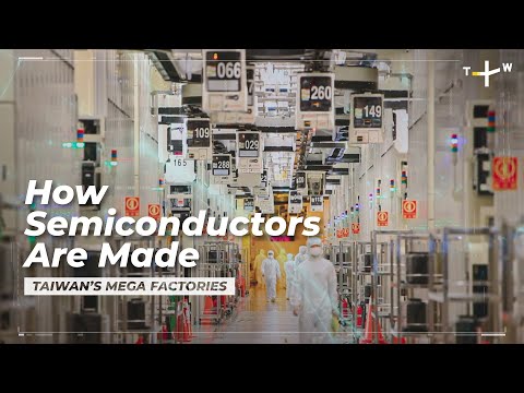
Inside Micron Taiwan’s Semiconductor Factory | Taiwan’s Mega Factories EP1
 0:04:53
TSMC's Shocking Chip Manufacturing Process EXPOSED!
 0:04:51
TSMC Announces the N3 FinFlex, N3E, and N2 Nodes, and 3DFabric
 0:09:19
【Chip】Unstoppable! TSMC's latest technology layout demonstrates the company's semiconducto...
 0:02:27
TSMC Launches Mass Production of 3-Nanometer Process | TaiwanPlus News
 0:04:13
How TSMC Plans to Expand The Chip Factory
 0:13:13
APPLE M2 / TSMC 2nm 3nm FINFLEX : L'avenir est en marche 💪 (Intel, AMD, Nvidia, CPU, GPU, AP...
![[Chip]Is it only](https://i.ytimg.com/vi/Jx4Mi78fO94/hqdefault.jpg) 0:08:28
0:08:28
[Chip]Is it only TSMC NO! How did Taiwan's chip design industry unknowingly become so powerful
 0:00:39
TMSC New 3nm Chip Processors Showing Performance & Density Improvements
 0:10:01
How Apple Changed TSMC - TSMC’s Success by Apple
 0:00:36
Apple unveils next-generation chip manufactured by Taiwan’s TSMC | TaiwanPlus News
 0:21:19
Record Wafer Prices: TSMC Financial Analysis, Q4 2022
 0:01:36
Snapdragon 8 Gen 4 to be made on TSMC N3E process, feature Phoenix Cores
 0:03:30
1.4 nm Is On The Horizon
 0:02:51
ijiweiTalk EP296: 3nm chips exclusive to apple, TSMC suffer losses?
 0:07:38
TSMC announces FINFLEX technology for its 3nm node in Bangla
 0:00:45
More Investment Firms Dump TSMC Shares | TaiwanPlus News
 0:01:34
Chinese Scholar: We Must Take Back Taiwan and Snatch Back TSMC, We Must Openly Support Russia
 0:00:42
TSMC Earnings Beat Expectations for Q2 | TaiwanPlus News
 0:02:10
TSMC | The Taiwan Firm That Makes the World’s Tech Run
 0:03:13
TSMC has 'tremendous' pricing power over its customers, says strategist
 0:02:53
TSMC expects 30% revenue growth in 2022 despite global uncertainties
 0:06:26
AMD Just Copied Intel! - TSMC Announces 2nm !
Комментарии