filmov
tv
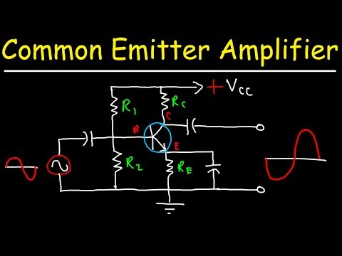
Design a Simple Common Emitter Amplifier

Показать описание
The common emitter amplifier is a simple single BJT circuit that can provide a reasonably large open circuit voltage gain (output is inverted). Learn how to design (i.e., choose resistor values) for a common emitter amplifier in order to get the gain that you require
David Williams
David Williams
 0:11:33
Design a Simple Common Emitter Amplifier
 0:08:26
Quick Guide: Designing A BJT Common Emitter Amplifier
 0:11:25
Bipolar Junction Transistors - Common Emitter Amplifier
 0:18:23
#273: Common Emitter Amplifier Design Tips & Shortcuts
 0:06:05
Design a Common Emitter Amplifier
 0:19:04
How to design a single transistor amplifier with voltage divider bias
 0:06:50
Design And Build A Common Emitter Amplifier
 0:22:17
Common Emitter Amplifier - Analysis and Design
 0:05:55
Single-Transistor Audio Amplifier - How the Common Emitter Amplifier Works
 0:28:32
Mastering Common-Emitter Transistor Amplifier Design: A Step-by-Step Guide!
 0:26:02
Designing a Common Emitter Configuration: NPN Transistor (For Amplifier)
 0:13:57
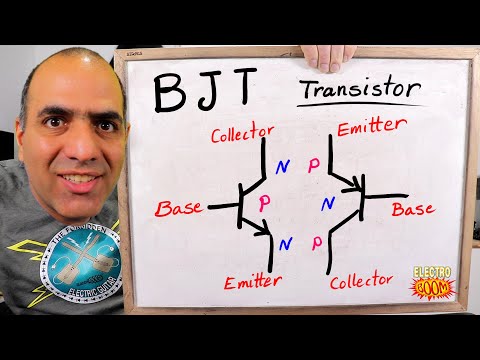
Starter Guide to BJT Transistors (ElectroBOOM101 - 011)
 0:35:49
Common Emitter Amplifier - Detailed Walkthrough - Simply Put
 0:01:00
Design a common emitter amplifier with this tricks..😮
 0:11:09
#114: Tutorial: Common Emitter, Common Collector, and Common Base Transistor amplifiers
 0:06:04
The Common Emitter Amplifier
 0:20:21
Common Emitter Amplifier - Theory and Basics (1/2)
 0:08:52
Design BJT Common Emitter Amplifier Using 7-Steps
 0:21:36
Common Emitter Amplifier
 0:18:46
Building the Common Emitter Amplifier
 0:57:53
Small Signal Amplifiers
 0:06:49
Design of Amplifier using BJT Part 1
 0:31:55
Tutorial for common-emitter amplifier design (part 1 of 2)
 0:03:49
Common Emitter ( CE ) amplifier in Proteus | Project file available for download
Комментарии