filmov
tv
AI’s Hardware Problem

Показать описание
Links:
 0:02:07
AI acceleration is a software problem | George Hotz and Lex Fridman
 0:11:34
AI’s Single Point of Failure | Rob Toews | TED
 0:15:24
AI Hardware, Explained.
 0:10:49
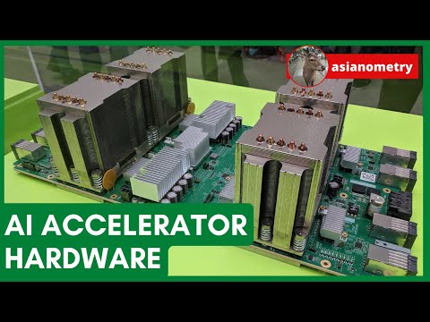
A Systematic Approach To Designing AI Accelerator Hardware
 0:14:05
'AI' Has A Huge Problem
 0:09:44
How AI is Killing Smartphones
 0:15:41
The Coming AI Chip Boom
 0:04:47
Steve Wozniak Reacts to Apple's New AI Tools
 0:02:41
SM2322 Portable SSD Controller: Suited for Next-Generation AI Smart Devices and Gaming Consoles
 0:22:12
I Had AI Troubleshoot Gaming PCs... Here's What Happened
 0:12:06
Google TPU & other in-house AI Chips
 0:08:49
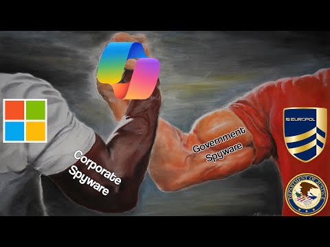
Microsoft's AI-Powered CoPilot+ PCs Are Spyware
 0:25:03
How AI Learned to Feel | 75 Years of Reinforcement Learning
 0:04:37
This new AI is powerful and uncensored… Let’s run it
 0:14:13
New Chinese AI Chips and their Huge Problems
 0:10:44
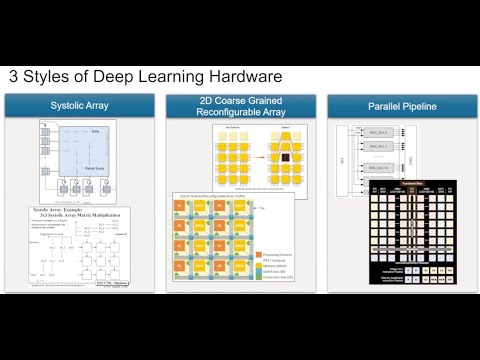
Different Types Of AI Hardware
 0:06:53
AI Hype: “Billions of dollars will be incinerated” Business Analysts Warn
 0:00:36
How much does an AI ENGINEER make?
 0:08:06
How much energy AI really needs. And why that's not its main problem.
 0:01:00
Why hasn't Apple invented this yet?!
 0:16:32
A.I. Expert Answers A.I. Questions From Twitter | Tech Support | WIRED
 0:05:49
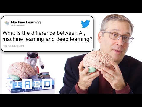
AI vs Machine Learning
 0:13:39
All The Jobs AI Will Replace In 5 Years (And Jobs That It Won’t)
 0:18:55
AI says why it will kill us all. Experts agree.
Комментарии