filmov
tv
Addressing Memory (Pt1) - Computerphile

Показать описание
Each BIT in memory doesn't have it's own unique wiring, they share connections - Dr 'Heartbleed' Bagley explains how we address them.
Memory Recall - COMING SOON
Professor Steve Furber on the ARM chip: COMING SOON, Subscribe for Updates!
Correction: In the graphic at 7min:30secs, a-0 & a-1 are incorrectly labelled a-1 & a-2
This video was filmed and edited by Sean Riley.
Memory Recall - COMING SOON
Professor Steve Furber on the ARM chip: COMING SOON, Subscribe for Updates!
Correction: In the graphic at 7min:30secs, a-0 & a-1 are incorrectly labelled a-1 & a-2
This video was filmed and edited by Sean Riley.
 0:08:20
Addressing Memory (Pt1) - Computerphile
 0:07:25
Total Recall (Memory Addressing Pt2) - Computerphile
 0:06:06
Why do CPUs Need Caches? - Computerphile
 0:09:04
The Fetch-Execute Cycle: What's Your Computer Actually Doing?
 0:08:22
Why Do We Need IP Addresses? - Computerphile
 0:08:54
Flip Flops, Latches & Memory Details - Computerphile
 0:10:50
Network Address Translation - Computerphile
 0:05:42
IP Addresses and the Internet - Computerphile
 0:17:37
The Path Towards ARM & BBC B - Computerphile
 0:19:49
Reverse Engineering - Computerphile
 0:14:49
OS Context Switching - Computerphile
 0:17:30
Running a Buffer Overflow Attack - Computerphile
 0:11:31
Where did Bytes Come From? - Computerphile
 0:12:51
Memory in a computer system
 0:14:04
A* (A Star) Search Algorithm - Computerphile
 0:09:36
Bus architecture and how register transfers work - 8 bit register - Part 1
 0:06:50
Email Endianness Problems - Computerphile
 0:06:41
Program, Interrupted - Computerphile
 0:10:00
35. OCR A Level (H446) SLR7 - 1.2 Addressing memory
 0:11:21
Origins of the Web - Computerphile
 0:11:55
Reflections on Trusting Trust - Computerphile
 0:04:55
The Computer That Changed Everything (Altair 8800) - Computerphile
 0:11:28
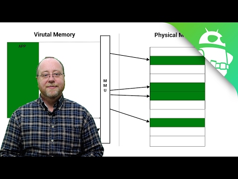
What is virtual memory? – Gary explains
 0:07:31
Colourspaces (JPEG Pt0)- Computerphile
Комментарии